


ADSP-2181/ADSP-2183
REV. 0
–16–
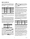
ADSP-2183–SPECIFICATIONS
RECOMMENDED OPERATING CONDITIONS
K Grade B Grade
Parameter Min Max Min Max Unit
V
DD
Supply Voltage 3.0 3.6 3.0 3.6 V
T
AMB
Ambient Operating Temperature 0 +70 –40 +85 °C
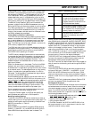
ELECTRICAL CHARACTERISTICS
K/B Grades
Parameter Test Conditions Min Max Unit
V
IH
Hi-Level Input Voltage
1, 2
@ V
DD
= max 2.0 V
V
IH
Hi-Level CLKIN Voltage @ V
DD
= max 2.2 V
V
IL
Lo-Level Input Voltage
1, 3
@ V
DD
= min 0.4 V
V
OH
Hi-Level Output Voltage
1, 4, 5
@ V
DD
= min
I
OH
= –0.5 mA 2.4 V
@ V
DD
= min
I
OH
= –100 µA
6
V
DD
– 0.3 V
V
OL
Lo-Level Output Voltage
1, 4, 5
@ V
DD
= min
I
OL
= 2 mA 0.4 V
I
IH
Hi-Level Input Current
3
@ V
DD
= max
V
IN
= V
DD
max 10 µA
I
IL
Lo-Level Input Current
3
@ V
DD
= max
V
IN
= 0 V 10 µA
I
OZH
Three-State Leakage Current
7
@ V
DD
= max,
V
IN
= V
DD
max
8
10 µA
I
OZL
Three-State Leakage Current
7
@ V
DD
= max,
V
IN
= 0 V
8
10 µA
I
DD
Supply Current (Idle)
9, 10
@ V
DD
= max, t
CK
= 34.7 ns 9 mA
I
DD
Supply Current (Dynamic)
10, 11
@ V
DD
= max
t
CK
= 34.7 ns
12
54 mA
C
I
Input Pin Capacitance
3, 6, 13
@ V
IN
= 2.5 V,
f
IN
= 1.0 MHz,
T
AMB
= +25°C8pF
C
O
Output Pin Capacitance
6, 7, 13, 14
@ V
IN
= 2.5 V,
f
IN
= 1.0 MHz,
T
AMB
= +25°C8pF
NOTES
1
Bidirectional pins: D0–D23, RFS0, RFS1, SCLK0, SCLK1, TFS0, TFS1, IAD0–IAD15, PF0–PF7.
2
Input only pins: RESET, IRQ2, BR, MMAP, DR0, DR1, PWD, IRQL0, IRQL1, IRQE, IS, IRD, IWR, IAL.
3
Input only pins: CLKIN, RESET, IRQ2, BR, MMAP, DR0, DR1, IS, IAL, IRD, IWR, IRQL0, IRQL1, IRQE, PWD.
4
Output pins: BG, PMS, DMS, BMS, IOMS, CMS, RD, WR, IACK, PWDACK, A0-A13, DT0, DT1, CLKOUT, FL2-0.
5
Although specified for TTL outputs, all ADSP-2183 outputs are CMOS-compatible and will drive to V
DD
and GND, assuming no dc loads.
6
Guaranteed but not tested.
7
Three-statable pins: A0–A13, D0–D23, PMS, DMS, BMS, IOMS, CMS, RD, WR, DT0, DT1, SCLK0, SCLK1, TFS0, TFS1, RFS0, RSF1, IAD0–IAD15, PF0–PF7.
8
0 V on BR, CLKIN Active (to force three-state condition).
9
Idle refers to ADSP-2183 state of operation during execution of IDLE instruction. Deasserted pins are driven to either V
DD
or GND.
10
Current reflects device operating with no output loads.
11
I
DD
measurement taken with all instructions executing from internal memory. 50% of the instructions are multifunction (types 1, 4, 5, 12, 13, 14), 30% are type 2
and type 6, and 20% are idle instructions.
12
V
IN
= 0.4 V and 2.4 V. For typical figures for supply currents, refer to “Power Dissipation” section.
13
Applies to TQFP and PQFP package types.
14
Output pin capacitance is the capacitive load for any three-stated output pin.
Specifications subject to change without notice.