


Chapter 4 45
POST Code Checkpoints
The Power-On Self Test (POST) is a BIOS procedure that boots the system, initializes and diagnoses the
system components, and controls the operation of the power-on password option. If POST discovers errors in
system operations at power-on, it displays error messages, generates a checkpoint code at port 80h or even
halts the system if the error is fatal.
The main components on the system board that must be diagnosed and/or initialized by POST to ensure
system functionality are as follows:
Microprocessor with built-in numeric coprocessor and cache memory subsystem
Direct memory access (DMA) controller (8237 module)
Interrupt system (8259 module)
Three programmable timers (system timer and 8254 module)
ROM subsystem
RAM subsystem
CMOS RAM subsystem and real time clock/calendar with battery backup
When POST executes a task, it uses a series of preset numbers called checkpoints to be latched at port 80h,
indicating the stages it is currently running. This latch can be read and shown on an external monitor
connected to the debug card.
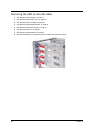
Viewing BIOS checkpoints
Viewing all checkpoints generated by the BIOS requires a debug card and an external monitor. Checkpoints
may appear on the bottom right corner of the screen during POST.
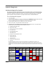
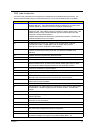
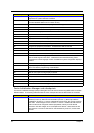
POST code checkpoints list
Bootblock initialization code checkpoint
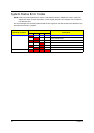
The following table describes the Award common tasks carried out by POST. An unique checkpoint number
denotes each task. .
Checkpoint Description
Before D1 Early chipset initialization is done. Early super I/O initialization is done including RTC
and keyboard controller. NMI is disabled.
D1 Perform keyboard controller BAT test. Check if waking up from power management
suspend state. Save power-on CPUID value in scratch CMOS.
D0 Go to flat mode with 4GB limit and GA20 enabled. Verify the bootblock checksum.
D2 Disable CACHE before memory detection. Execute full memory sizing module.
Verify that flat mode is enabled.
D3 If memory sizing module not executed, start memory refresh and do memory sizing in
Bootblock code. Do additional chipset initialization. Re-enable CACHE. Verify that
flat mode is enabled.
D4 Test base 512KB memory. Adjust policies and cache first 8MB. Set stack.
D5 Bootblock code is copied from ROM to lower system memory and control is given to
it. BIOS now executes out of RAM.
D6 Both key sequence and OEM specific method is checked to determine if BIOS
recovery is forced. Main BIOS checksum is tested. If BIOS recovery is necessary,
control flows to checkpoint E0. See Bootblock Recovery Code Checkpoints section
of document for more information.