


ADVANCE
CY14E108L, CY14E108N
Document Number: 001-45524 Rev. *A Page 5 of 20
Software STORE
Transfer data from the SRAM to the nonvolatile memory with a
software address sequence. The CY14B108L/CY14B108N
software STORE cycle is initiated by executing sequential CE
controlled READ cycles from six specific address locations in
exact order. During the STORE cycle an erase of the previous
nonvolatile data is first performed, followed by a program of the
nonvolatile elements. After a STORE cycle is initiated, further
input and output are disabled until the cycle is completed.
Because a sequence of READs from specific addresses is used
for STORE initiation, it is important that no other READ or WRITE
accesses intervene in the sequence. If there are intervening
READ or WRITE accesses, the sequence is aborted and no
STORE or RECALL takes place.
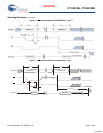
To initiate the software STORE cycle, the following READ
sequence must be performed.
1. Read Address 0x4E38 Valid READ
2. Read Address 0xB1C7 Valid READ
3. Read Address 0x83E0 Valid READ
4. Read Address 0x7C1F Valid READ
5. Read Address 0x703F Valid READ
6. Read Address 0x8FC0 Initiate STORE Cycle
The software sequence may be clocked with CE
controlled
READs or OE
controlled READs. After the sixth address in the
sequence is entered, the STORE cycle commences and the chip
is disabled. It is important to use READ cycles and not WRITE
cycles in the sequence, although it is not necessary that OE be
LOW for a valid sequence. After the t
STORE
cycle time is fulfilled,
the SRAM is activated again for the READ and WRITE operation.
Software RECALL
Transfer the data from the nonvolatile memory to the SRAM with
a software address sequence. A software RECALL cycle is
initiated with a sequence of READ operations in a manner similar
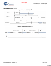
to the software STORE initiation. To initiate the RECALL cycle,
the following sequence of CE
controlled READ operations must
be performed.
1. Read Address 0x4E38 Valid READ
2. Read Address 0xB1C7 Valid READ
3. Read Address 0x83E0 Valid READ
4. Read Address 0x7C1F Valid READ
5. Read Address 0x703F Valid READ
6. Read Address 0x4C63 Initiate RECALL Cycle
Internally, RECALL is a two step procedure. First, the SRAM data
is cleared and then the nonvolatile information is transferred into
the SRAM cells. After the t
RECALL
cycle time, the SRAM is again
ready for READ and WRITE operations. The RECALL operation
does not alter the data in the nonvolatile elements.
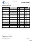
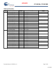
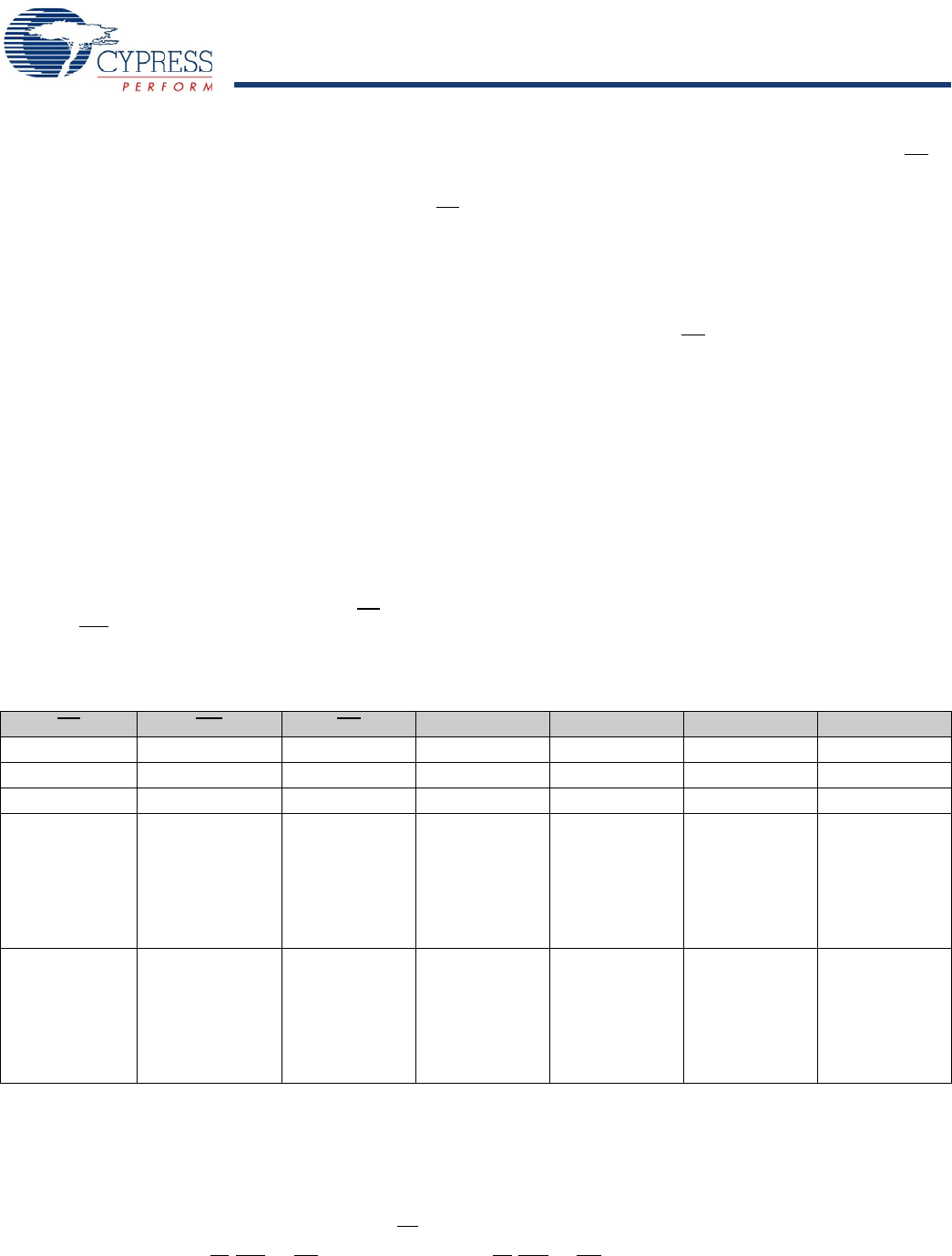
Table 1. Mode Selection
CE WE OE
A15 - A0 Mode IO Power
H X X X Not Selected Output High Z Standby
L H L X Read SRAM Output Data Active
L L X X Write SRAM Input Data Active
L H L 0x4E38
0xB1C7
0x83E0
0x7C1F
0x703F
0x8B45
Read SRAM
Read SRAM
Read SRAM
Read SRAM
Read SRAM
AutoStore
Disable
Output Data
Output Data
Output Data
Output Data
Output Data
Output Data
Active
[3,4,5]
L H L 0x4E38
0xB1C7
0x83E0
0x7C1F
0x703F
0x4B46
Read SRAM
Read SRAM
Read SRAM
Read SRAM
Read SRAM
AutoStore Enable
Output Data
Output Data
Output Data
Output Data
Output Data
Output Data
Active
[3,4,5]
Notes
3. The six consecutive address locations must be in the order listed. WE
must be HIGH during all six cycles to enable a nonvolatile cycle.
4. While there are 20/19 address lines on the CY14B108L/CY14B108N, only the lower 16 lines are used to control software modes.
5. IO state depends on the state of OE
, BHE, and BLE. The IO table shown assumes OE, BHE, and BLE LOW.
[+] Feedback