


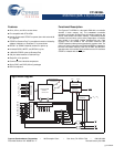
CY14E256L
Document Number: 001-06968 Rev. *F Page 6 of 18
Best Practices
nvSRAM products have been used effectively for over 15 years.
While ease of use is one of the product’s main system values,
experience gained working with hundreds of applications has
resulted in the following suggestions as best practices:
■
The nonvolatile cells in an nvSRAM are programmed on the
test floor during final test and quality assurance. Incoming
inspection routines at customer or contract manufacturer’s
sites sometimes reprogram these values. Final NV patterns are
typically repeating patterns of AA, 55, 00, FF, A5, or 5A. End
product’s firmware should not assume an NV array is in a set
programmed state. Routines that check memory content
values to determine first time system configuration, cold or
warm boot status, and so on should always program a unique
NV pattern (for example, complex 4-byte pattern of 46 E6 49
53 hex or more random bytes) as part of the final system
manufacturing test to ensure these system routines work
consistently.
■
Power up boot firmware routines should rewrite the nvSRAM
into the desired state. While the nvSRAM is shipped in a preset
state, best practice is to again rewrite the nvSRAM into the
desired state as a safeguard against events that might flip the
bit inadvertently (program bugs, incoming inspection routines,
and so on).
■
The V
CAP
value specified in this data sheet includes a minimum
and a maximum value size. Best practice is to meet this
requirement and not exceed the maximum V
CAP
value because
the higher inrush currents may reduce the reliability of the
internal pass transistor. Customers that want to use a larger
V
CAP
value to make sure there is extra store charge should
discuss their V
CAP
size selection with Cypress to understand
any impact on the V
CAP
voltage level at the end of a t
RECALL
period.
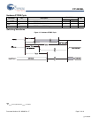
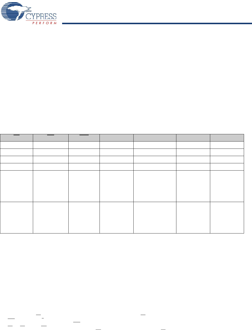
Table 1. Hardware Mode Selection
CE WE HSB A13–A0 Mode IO Power
H X H X Not Selected Output High Z Standby
L H H X Read SRAM Output Data Active
[1]
L L H X Write SRAM Input Data Active
X X L X Nonvolatile STORE Output High Z I
CC2
[2]
LHH0x0E38
0x31C7
0x03E0
0x3C1F
0x303F
0x0FC0
Read SRAM
Read SRAM
Read SRAM
Read SRAM
Read SRAM
Nonvolatile STORE
Output Data
Output Data
Output Data
Output Data
Output Data
Output High Z
Active
[1, 3, 4, 5]
I
CC2
LHH0x0E38
0x31C7
0x03E0
0x3C1F
0x303F
0x0C63
Read SRAM
Read SRAM
Read SRAM
Read SRAM
Read SRAM
Nonvolatile RECALL
Output Data
Output Data
Output Data
Output Data
Output Data
Output High Z
Active
[1, 3, 4, 5]
Notes
1. I/O state assumes OE
< V
IL
. Activation of nonvolatile cycles does not depend on state of OE.
2. HSB
STORE operation occurs only if an SRAM WRITE has been done since the last nonvolatile cycle. After the STORE (if any) completes, the part goes into
standby mode, inhibiting all operations until HSB
rises.
3. CE
and OE LOW and WE HIGH for output behavior.
4. The six consecutive addresses must be in the order listed. WE
must be high during all six consecutive CE controlled cycles to enable a nonvolatile cycle.
5. While there are 15 addresses on the CY14E256L, only the lower 14 are used to control software modes.
[+] Feedback