CY2309NZ
Document #: 38-07182 Rev. *E Page 2 of 6
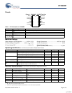
Pinouts
Figure 1. CY2309NZ - 16 SOIC-Top View
Maximum Ratings
Supply Voltage to Ground Potential................–0.5V to +7.0V
DC Input Voltage (Except REF) ............–0.5V to V
DD
+ 0.5V
DC Input Voltage REF .........................................–0.5V to 7V
Storage Temperature .................................–65°C to +150°C
Junction Temperature................................................. 150°C
Static Discharge Voltage
(per MIL-STD-883, Method 3015) ............................>2,000V
1
2
3
4
5
6
7
8
9
10
11
12
13
14
15
16
BUF_IN
OUTPUT1
OUTPUT2
V
DD
GND
OUTPUT3
OUTPUT4
V
DD
OUTPUT9
OUTPUT8
OUTPUT7
V
DD
GND
OUTPUT6
OUTPUT5
GND
Table 1. Pin Description for CY2309NZ
Pin Signal Description
4, 8, 13 V
DD
3.3V Digital Voltage Supply
5, 9, 12 GND Ground
1 BUF_IN Input Clock
2, 3, 6, 7, 10,
11, 14, 15, 16
OUTPUT [1:9] Outputs
Operating Conditions for Commercial and Industrial Temperature Devices
Parameter Description Min Max Unit
V
DD
Supply Voltage 3.0 3.6 V
T
A
(Ambient Operating Temperature) Commercial 0 70 °C
(Ambient Operating Temperature) Industrial –40 85
°C
C
L
Load Capacitance, Fout < 100 MHz 30 pF
Load Capacitance,100 MHz < Fout < 133.33 MHz 15 pF
C
IN
Input Capacitance 7 pF
BUF_IN, OUTPUT [1:9] Operating Frequency DC 133.33 MHz
t
PU
Power up time for all VDDs to reach minimum specified
voltage (power ramps must be monotonic)
0.05 50 ms
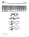
Electrical Characteristics for Commercial and Industrial Temperature Devices
Parameter Description Test Conditions Min Max Unit
V
IL
Input LOW Voltage
[1]
0.8 V
V
IH
Input HIGH Voltage
[1]
2.0 V
I
IL
Input LOW Current V
IN
= 0V 50.0 μA
I
IH
Input HIGH Current V
IN
= V
DD
100.0 μA
V
OL
Output LOW Voltage
[2]
I
OL
= 8 mA 0.4 V
V
OH
Output HIGH Voltage
[2]
I
OH
= –8 mA 2.4 V
I
DD
Supply Current Unloaded outputs at 66.66 MHz 32 mA
Notes
1. BUF_IN input has a threshold voltage of V
DD
/2.
2. Parameter is guaranteed by design and characterization. It is not 100% tested in production.
[+] Feedback


