CY25822
-2
Document #: 38-07531 Rev. ** Page 3 of 9
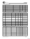
.... Data Byte N –8 bits 56 Acknowledge
.... Acknowledge from slave .... Data bytes from slave/Acknowledge
.... Stop .... Data byte N from slave – 8 bits
.... Not Acknowledge
.... Stop
Table 2. Block Read and Block Write Protocol (continued)
Table 3. Byte Read and Byte Write Protocol
Byte Write Protocol Byte Read Protocol
Bit Description Bit Description
1Start 1Start
2:8 Slave address – 7 bits 2:8 Slave address – 7 bits
9 Write = 0 9 Write = 0
10 Acknowledge from slave 10 Acknowledge from slave
11:18 Command Code – 8 bits
'1xxxxxxx' stands for byte operation, bits[6:0] of
the command code represents the offset of the
byte to be accessed
11:18 Command Code – 8 bits
'1xxxxxxx' stands for byte operation, bits[6:0]
of the command code represents the offset of
the byte to be accessed
19 Acknowledge from slave 19 Acknowledge from slave
20:27 Data byte from master – 8 bits 20 Repeat start
28 Acknowledge from slave 21:27 Slave address – 7 bits
29 Stop 28 Read = 1
29 Acknowledge from slave
30:37 Data byte from slave – 8 bits
38 Not Acknowledge
39 Stop
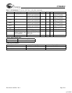
Byte 0: Control Register
Bit @Pup Pin# Name Pin Description
714SS0 –
604SS1 –
504SS2 –
404SS3 –
3 1 Not Applicable Reserved, must be written as 1
214, 5CLKOUT,
REFOUT
Power-down three-state enable
0 = three-state outputs, 1 = drive outputs low
(Applies only in Power Down State)
1 1 4 CLKOUT Spread Spectrum enable
0 = spread off, 1 = spread on
0 0 Not Applicable No Pins
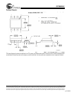
Table 4. Spread Spectrum Select
SS3 SS2 SS1 SS0 Spread Mode Spread Amount%
0 0 0 0 Down 0.8
0 0 0 1 Down 1.0
0 0 1 0 Down 1.25
0 0 1 1 Down 1.5
0 1 0 0 Down 1.75
[+] Feedback


