


CY62147DV30
Document #: 38-05340 Rev. *F Page 4 of 12
Notes:
10. Tested initially and after any design or process changes that may affect these parameters.
11.Test condition for the 45-ns part is a load capacitance of 30 pF.
12.Full device operation requires linear V
CC
ramp from V
DR
to V
CC(min.)
> 100 µs or stable at V
CC(min.)
> 100 µs.
13.BHE
.BLE is the AND of both BHE and BLE. Chip can be deselected by either disabling the chip enable signals or by disabling both BHE and BLE.
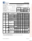
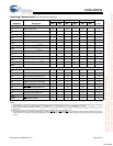
Capacitance (for all packages)
[10]
Parameter Description Test Conditions Max. Unit
C
IN
Input Capacitance T
A
= 25°C, f = 1 MHz,
V
CC
= V
CC(typ)
10 pF
C
OUT
Output Capacitance 10 pF
Thermal Resistance
[10]
Parameter Description Test Conditions VFBGA TSOP II Unit
Θ
JA
Thermal Resistance
(Junction to Ambient)
Still Air, soldered on a 3 × 4.5 inch, four-layer
printed circuit board
72 75.13 °C/W
Θ
JC
Thermal Resistance
(Junction to Case)
8.86 8.95 °C/W
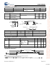
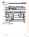
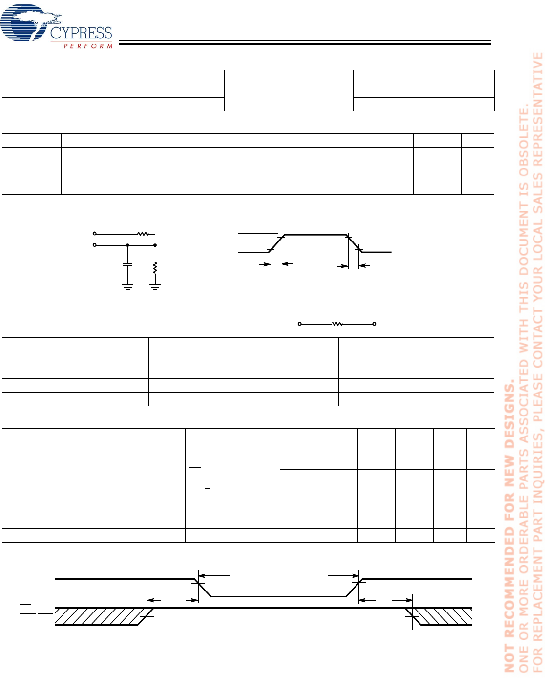
AC Test Loads and Waveforms
[10]
Parameters 2.50V 3.0V Unit
R1 16667 1103 Ω
R2 15385 1554 Ω
R
TH
8000 645 Ω
V
TH
1.20 1.75 V
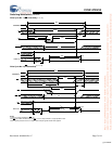
Data Retention Characteristics (Over the Operating Range)
Parameter Description Conditions Min. Typ.
[5]
Max. Unit
V
DR
V
CC
for Data Retention 1.5 V
I
CCDR
Data Retention Current V
CC
= 1.5V
CE
> V
CC
– 0.2V,
V
IN
> V
CC
– 0.2V or
V
IN
< 0.2V
L (Auto-E) 15 µA
LL (Ind’l/Auto-A) 6
t
CDR
[10]
Chip Deselect to Data Retention
Time
0 ns
t
R
[12]
Operation Recovery Time t
RC
ns
V
CC
V
CC
OUTPUT
R2
50 pF
INCLUDING
JIG AND
SCOPE
GND
90%
10%
90%
10%
Rise Time = 1 V/ns
Fall Time = 1 V/ns
OUTPUT V
Equivalent to: THÉ VENIN EQUIVALENT
ALL INPUT PULSES
R
TH
R1
Data Retention Waveform
[13]
V
CC(min)
V
CC(min)
t
CDR
V
DR
> 1.5 V
DATA RETENTION MODE
t
R
V
CC
CE or
BHE
.BLE
[+] Feedback