


CY62157EV30 MoBL
®
Document #: 38-05445 Rev. *E Page 6 of 14
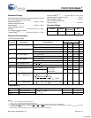
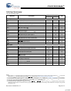
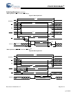
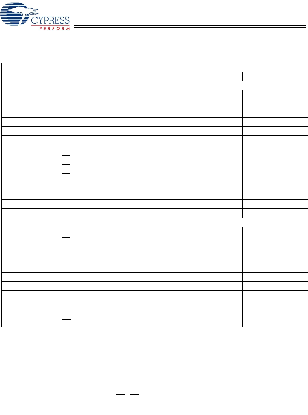
Switching Characteristics
Over the Operating Range
[13, 14]
Parameter Description
45 ns (Ind’l/Auto-A)
Unit
Min Max
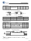
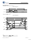
Read Cycle
t
RC
Read Cycle Time 45 ns
t
AA
Address to Data Valid 45 ns
t
OHA
Data Hold from Address Change 10 ns
t
ACE
CE
1
LOW and CE
2
HIGH to Data Valid 45 ns
t
DOE
OE LOW to Data Valid 22 ns
t
LZOE
OE LOW to LOW-Z
[15]
5ns
t
HZOE
OE HIGH to High-Z
[15, 16]
18 ns
t
LZCE
CE
1
LOW and CE
2
HIGH to Low-Z
[15]
10 ns
t
HZCE
CE
1
HIGH and CE
2
LOW to High-Z
[15, 16]
18 ns
t
PU
CE
1
LOW and CE
2
HIGH to Power Up 0 ns
t
PD
CE
1
HIGH and CE
2
LOW to Power Down 45 ns
t
DBE
BLE/BHE LOW to Data Valid 45 ns
t
LZBE
BLE/BHE LOW to Low-Z
[15, 17]
5ns
t
HZBE
BLE/BHE HIGH to HIGH-Z
[15, 16]
18 ns
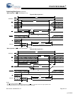
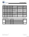
Write Cycle
[18]
t
WC
Write Cycle Time 45 ns
t
SCE
CE
1
LOW and CE
2
HIGH
to Write End 35 ns
t
AW
Address Setup to Write End 35 ns
t
HA
Address Hold from Write End 0 ns
t
SA
Address Setup to Write Start 0 ns
t
PWE
WE Pulse Width 35 ns
t
BW
BLE/BHE LOW to Write End 35 ns
t
SD
Data Setup to Write End 25 ns
t
HD
Data Hold from Write End 0 ns
t
HZWE
WE LOW to High-Z
[15, 16]
18 ns
t
LZWE
WE HIGH to Low-Z
[15]
10 ns
Notes
13. Test conditions for all parameters other than tri-state parameters assume signal transition time of 3 ns or less, timing reference levels of V
CC(typ)
/2, input pulse
levels of 0 to V
CC(typ)
, and output loading of the specified I
OL
/I
OH
as shown in the “AC Test Loads and Waveforms” on page 5.
14. AC timing parameters are subject to byte enable signals (BHE
or BLE) not switching when chip is disabled. See application note AN13842 for further clarification.
15. At any temperature and voltage condition, t
HZCE
is less than t
LZCE
, t
HZBE
is less than t
LZBE
, t
HZOE
is less than t
LZOE
, and t
HZWE
is less than t
LZWE
for any device.
16. t
HZOE
, t
HZCE
, t
HZBE
, and t
HZWE
transitions are measured when the outputs enter a high-impedance state.
17. If both byte enables are toggled together, this value is 10 ns.
18. The internal write time of the memory is defined by the overlap of WE
, CE
= V
IL
, BHE, BLE or both = V
IL
, and CE
2
= V
IH
. All signals must be active to initiate a
write and any of these signals can terminate a write by going inactive. The data input setup and hold timing must be referenced to the edge of the signal that
terminates the write.
[+] Feedback