CY62167E MoBL
®
Document #: 001-15607 Rev. *A Page 2 of 12
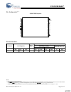
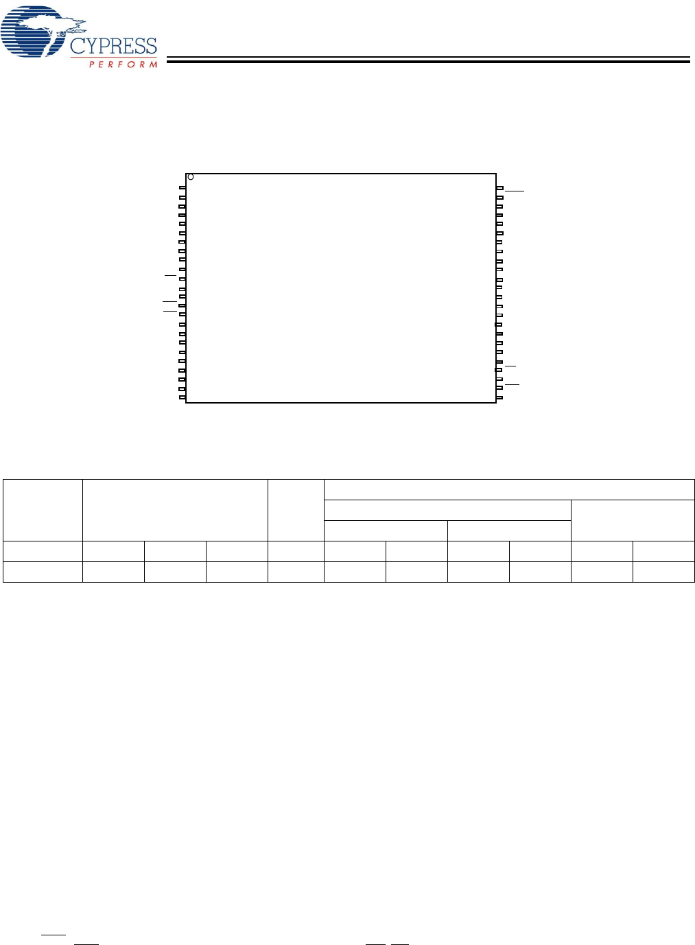
Pin Configuration
[2, 3]
48-Pin TSOP I Top View
Product Portfolio
Product V
CC
Range (V)
Speed
(ns)
Power Dissipation
Operating I
CC
(mA)
Standby I
SB2
(µA)
f = 1 MHz f = f
max
Min Typ
[4]
Max Typ
[4]
Max Typ
[4]
Max Typ
[4]
Max
CY62167ELL 4.5 5.0 5.5 45 2.2 4.0 25 30 1.5 12
1
2
3
4
5
6
7
8
9
10
11
12
13
14
15
16
17
18
19
20
21
22
23
24
48
47
46
45
44
43
42
41
40
39
38
37
36
35
34
33
32
31
30
29
28
27
26
25
A15
A14
A13
A12
A11
A10
A9
A8
A19
NC
WE
CE
2
NC
BHE
BLE
A18
A17
A7
A6
A5
A4
A3
A2
A1
A16
BYTE
Vss
IO15/A20
IO7
IO14
IO6
IO13
IO5
IO12
IO4
Vcc
IO11
IO3
IO10
IO2
IO9
IO1
IO8
IO0
OE
Vss
CE1
A0
Notes
2. NC pins are not connected on the die.
3. The BYTE
pin in the 48-TSOPI package must be tied to V
CC
to use the device as a 1M X 16 SRAM. The 48-TSOPI package can also be used as a 2M X 8 SRAM
by tying the BYTE signal to V
SS
. In the 2M x 8 configuration, pin 45 is A20, while BHE, BLE and IO
8
to IO
14
pins are not used.
4. Typical values are included for reference only and are not guaranteed or tested. Typical values are measured at V
CC
= V
CC
(typ), T
A
= 25°C.
[+] Feedback [+] Feedback [+] Feedback


