


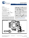

CY62167EV18 MoBL
®
Document #: 38-05447 Rev. *G Page 4 of 13
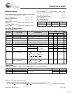
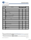
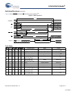
Thermal Resistance
Tested initially and after any design or process changes that may affect these parameters.
Parameter Description Test Conditions
VFBGA
(6 x 7 x 1mm)
VFBGA
(6 x 8 x 1mm)
Unit
Θ
JA
Thermal Resistance
(Junction to Ambient)
Still air, soldered on a 3 × 4.5 inch,
two-layer printed circuit board
27.74 55 °C/W
Θ
JC
Thermal Resistance
(Junction to Case)
9.84 16 °C/W
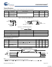
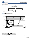
Figure 2. AC Test Loads and Waveforms
Parameters 1.8V Unit
R1 13500 Ω
R2 10800 Ω
R
TH
6000 Ω
V
TH
0.80 V
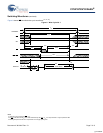
Data Retention Characteristics
Over the Operating Range
Parameter Description Conditions Min Typ
[4]
Max Unit
V
DR
V
CC
for Data Retention 1.0 V
I
CCDR
[9]
Data Retention Current V
CC
= 1.0V, CE
1
> V
CC
– 0.2V, CE
2
< 0.2V,
V
IN
> V
CC
– 0.2V or V
IN
< 0.2V
10 μA
t
CDR
[10]
Chip Deselect to Data
Retention Time
0ns
t
R
[11]
Operation Recovery Time t
RC
ns
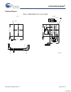
Figure 3. Data Retention Waveform
V
CC
V
CC
OUTPUT
R2
30 pF
INCLUDING
JIG AND
SCOPE
GND
90%
10%
90%
10%
Rise Time = 1 V/ns
Fall Time = 1 V/ns
OUTPUT V
Equivalent to: THÉVENIN EQUIVALENT
ALL INPUT PULSES
R
TH
R1
Notes
10.Tested initially and after any design or process changes that may affect these parameters.
11. Full device operation requires linear V
CC
ramp from V
DR
to V
CC
(min) > 100 μs or stable at V
CC
(min) > 100 μs.
12.BHE
.BLE is the AND of both BHE and BLE. Deselect the chip by either disabling the chip enable signals or by disabling both BHE and BLE.
V
CC
(min)
V
CC
(min)
t
CDR
V
DR
>
1.0 V
DATA RETENTION MODE
t
R
CE
1
or
V
CC
BHE.BLE
CE
2
or
[12]
[+] Feedback