


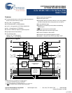
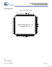
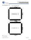
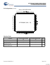
CY7C024AV/024BV/025AV/026AV
CY7C0241AV/0251AV/036AV
Document #: 38-06052 Rev. *J Page 8 of 19
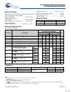
Maximum Ratings
Exceeding maximum ratings
[14]
may shorten the useful life of the
device. User guidelines are not tested.
Storage Temperature ................................. –65°C to +150°C
Ambient Temperature with
Power Applied ............................................ –55°C to +125°C
Supply Voltage to Ground Potential............... –0.5V to +4.6V
DC Voltage Applied to
Outputs in High-Z State .........................–0.5V to V
CC
+ 0.5V
DC Input Voltage
[15]
............................... –0.5V to V
CC
+ 0.5V
Output Current into Outputs (LOW).............................20 mA
Static Discharge Voltage.......................................... > 2001V
Latch-up Current.................................................... > 200 mA
Operating Range
Range Ambient Temperature V
CC
Commercial 0°C to +70°C 3.3V ± 300 mV
Industrial
[16]
–40°C to +85°C 3.3V ± 300 mV
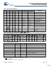
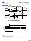
Electrical Characteristics
Over the Operating Range
Parameter Description
CY7C024AV/024BV/025AV/026AV
CY7C0241AV/0251AV/036AV
Unit
-20 -25
Min Typ Max Min Typ Max
V
OH
Output HIGH Voltage (V
CC
=3.3V) 2.4 2.4 V
V
OL
Output LOW Voltage 0.4 0.4 V
V
IH
Input HIGH Voltage 2.0 2.0 V
V
IL
Input LOW Voltage –0.3
[17]
0.8 0.8 V
I
OZ
Output Leakage Current –10 10 –10 10 μA
I
IX
Input Leakage Current –10 10 –10 10 μA
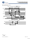
I
CC
Operating Current (V
CC
= Max.,
I
OUT
= 0 mA) Outputs Disabled
Com’l. 120 175 115 165 mA
Ind.
[16]
135 185 mA
I
SB1
Standby Current (Both Ports TTL Level)
CE
L
& CE
R
≥ V
IH
, f = f
MAX
Com’l. 35 45 30 40 mA
Ind.
[16]
40 50 mA
I
SB2
Standby Current (One Port TTL Level)
CE
L
| CE
R
≥ V
IH
, f = f
MAX
Com’l. 75 110 65 95 mA
Ind.
[16]
75 105 mA
I
SB3
Standby Current (Both Ports CMOS Level)
CE
L
& CE
R
≥ V
CC
−0.2V, f = 0
Com’l. 10 500 10 500 μA
Ind.
[16]
10 500 μA
I
SB4
Standby Current (One Port CMOS Level)
CE
L
| CE
R
≥ V
IH
, f = f
MAX
[18]
Com’l. 70 95 60 80 mA
Ind.
[16]
70 90 mA
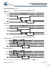
Capacitance
Parameter
[19]
Description Test Conditions Max Unit
C
IN
Input Capacitance T
A
= 25
°
C, f = 1 MHz,
V
CC
= 3.3V
10 pF
C
OUT
Output Capacitance 10 pF
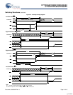
Notes
14.The voltage on any input or IO pin cannot exceed the power pin during power up.
15.Pulse width < 20 ns.
16.Industrial parts are available in CY7C026AV and CY7C036AV only.
17.VIL >
–1.5V for pulse width less than 10ns.
18.f
MAX
= 1/t
RC
= All inputs cycling at f = 1/t
RC
(except output enable). f = 0 means no address or control lines change. This applies only to inputs at CMOS level
standby I
SB3
.
19.Tested initially and after any design or process changes that may affect these parameters.
[+] Feedback