CY7C09079V/89V/99V
CY7C09179V/89V/99V
Document #: 38-06043 Rev. *C Page 10 of 21
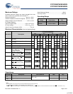
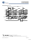
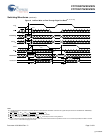
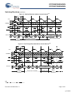
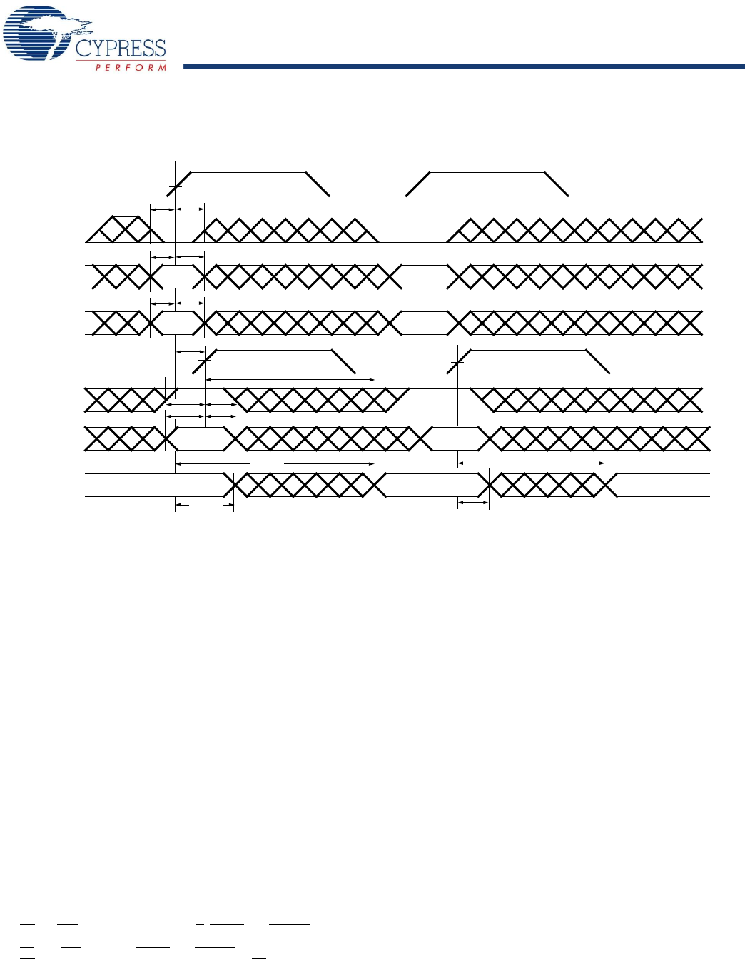
Figure 9. Left Port Write to Flow-Through Right Port Read
[22, 23, 24, 25]
Notes
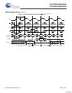
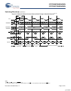
20. In this depth expansion example, B1 represents Bank #1 and B2 is Bank #2; Each Bank consists of one Cypress dual-port device from this datasheet. ADDRESS
(B1)
= ADDRESS
(B2)
.
21.OE
and ADS = V
IL
; CE
1(B1)
, CE
1(B2)
, R/W, CNTEN, and CNTRST = V
IH
.
22.The same waveforms apply for a right port write to flow-through left port read.
23.CE
0
and ADS = V
IL
; CE
1
, CNTEN, and CNTRST = V
IH
.
24.OE
= V
IL
for the right port, which is being read from. OE = V
IH
for the left port, which is being written to.
25.It t
CCS
≤ maximum specified, then data from right port READ is not valid until the maximum specified for t
CWDD
. If t
CCS
>maximum specified, then data is not valid
until t
CCS
+ t
CD1
. t
CWDD
does not apply in this case.
Switching Waveforms (continued)
t
SA
t
HA
t
SW
t
HW
t
SD
t
HD
MATCH
VALID
t
CCS
t
SW
t
HW
t
DC
t
CWDD
t
CD1
MATCH
t
SA
t
HA
MATCH
NO
MATCH
NO
VALID VALID
t
DC
t
CD1
CLK
L
R/W
L
ADDRESS
L
DATA
INL
ADDRESS
R
DATA
OUTR
CLK
R
R/W
R
[+] Feedback


