CY7C1166V18, CY7C1177V18
CY7C1168V18, CY7C1170V18
Document Number: 001-06620 Rev. *D Page 6 of 27
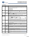
Pin Definitions
Pin Name IO Pin Description
DQ
[x:0]
Input Output-
Synchronous
Data Input Output Signals. Inputs are sampled on the rising edge of K and K clocks during valid
write operations. These pins drive out the requested data when a read operation is active. Valid data
is driven out on the rising edge of both the K and K clocks during read operations. When read access
is deselected, Q[x:0] are automatically tri-stated.
CY7C1166V18 − DQ
[7:0]
CY7C1177V18 − DQ
[8:0]
CY7C1168V18 − DQ
[17:0]
CY7C1170V18 − DQ
[35:0]
LD Input-
Synchronous
Synchronous Load. This input is brought LOW when a bus cycle sequence is to be defined. This
definition includes address and read/write direction. All transactions operate on a burst of two data.
LD
must meet the setup and hold times around edge of K. LD must meet the setup and hold times
around edge of K.
NWS
0
, NWS
1
, Input-
Synchronous
Nibble Write Select 0, 1 − Active LOW.(CY7C1166V18 Only) Sampled on the rising edge of the K
and K
clocks during write operations. It is used to select the nibble that is written into the device
NWS
0
controls D
[3:0]
and NWS
1
controls D
[7:4]
.
All the Nibble Write Selects are sampled on the same edge as the data. Deselecting a Nibble Write
Select ignores the corresponding nibble of data and not written into the device.
BWS
0
,
BWS
1
,
BWS
2
, BWS
3
Input-
Synchronous
Byte Write Select 0, 1, 2, and 3 − Active LOW. Sampled on the rising edge of the K and K clocks
during Write operations. It is used to select the byte that is written into the device during the current
portion of the write operations. Bytes not written remain unaltered.
CY7C1177V18 − BWS
0
controls D
[8:0]
CY7C1168V18 − BWS
0
controls D
[8:0],
and BWS
1
controls D
[17:9].
CY7C1170V18 − BWS
0
controls D
[8:0]
, BWS
1
controls D
[17:9]
, BWS
2
controls D
[26:18]
, and BWS
3
controls D
[35:27]
.
All the Byte Write Selects are sampled on the same edge as the data. Deselecting a Byte Write Select
ignores the corresponding byte of data and not written into the device.
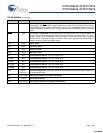
A Input-
Synchronous
Address Inputs. Sampled on the rising edge of the K clock during active read and write operations.
These address inputs are multiplexed for both read and write operations. Internally, the device is
organized as 2M x 8 (two arrays each of1M x 8) for CY7C1166V18, 2M x 9 (two arrays each of 1M
x 9) for CY7C1177V18, 1M x 18 (two arrays each of 512K x 18) for CY7C1168V18, and 512K x 36
(two arrays each of 256K x 18) for CY7C1170V18. All the address inputs are ignored when the
appropriate port is deselected.
R/W
Input-
Synchronous
Synchronous Read/Write Input. When LD
is LOW, this input designates the access type (read
when R/W
is HIGH, write when R/W is LOW) for loaded address. R/W must meet the setup and hold
times around edge of K.
QVLD Valid Output
Indicator
Valid Output Indicator. The Q Valid indicates valid output data. QVLD is edge aligned with CQ and
CQ
.
K Input-
Clock
Positive Input Clock Input. The rising edge of K is used to capture synchronous inputs to the device
and to drive out data through Q
[x:0]
when in single clock mode. All accesses are initiated on the rising
edge of K.
K
Input-
Clock
Negative Input Clock Input. K is used to capture synchronous inputs being presented to the device
and to drive out data through Q
[x:0]
when in single clock mode.
CQ Clock Output Synchronous Echo Clock Outputs. This is a free running clock and is synchronized to the input
clock (K) of the DDR-II+. The timings for the echo clocks are shown in the “Switching Characteristics”
on page 22.
CQ
Clock Output
Synchronous Echo Clock Outputs. This is a free running clock and is synchronized to the input
clock (K) of the DDR-II+. The timings for the echo clocks are shown in the “Switching Characteristics”
on page 22.
[+] Feedback [+] Feedback


