CY7C1306BV25
CY7C1303BV25
Document #: 38-05627 Rev. *A Page 5 of 19
Introduction
Functional Overview
The CY7C1303BV25/CY7C1306BV25 are synchronous
pipelined Burst SRAM equipped with both a Read port and a
Write port. The Read port is dedicated to Read operations and
the Write port is dedicated to Write operations. Data flows into
the SRAM through the Write port and out through the Read
port. These devices multiplex the address inputs in order to
minimize the number of address pins required. By having
separate Read and Write ports, this architecture completely
eliminates the need to “turn-around” the data bus and avoids
any possible data contention, thereby simplifying system
design. 38-05627Each access consists of two 18-bit data
transfers in the case of CY7C1303BV25, and two 36-bit data
transfers in the case of CY7C1306BV25, in one clock cycle.
Accesses for both ports are initiated on the rising edge of the
Positive Input Clock (K). All synchronous input timing is refer-
enced from the rising edge of the input clocks (K and K
) and
all output timings are referenced to rising edge of output clocks
(C and C
or K and K when in single clock mode).
All synchronous data inputs (D
[x:0]
) pass through input
registers controlled by the rising edge of the input clocks (K
and K
). All synchronous data outputs (Q
[x:0]
) pass through
output registers controlled by the rising edge of the output
clocks (C and C
, or K and K when in single clock mode).
All synchronous control (RPS
, WPS, BWS
[x:0]
) inputs pass
through input registers controlled by the rising edge of input
clocks (K and K
).
The following descriptions take CY7C1303BV25 as an
example. The same basic descriptions apply to
CY7C1306BV25.
Read Operations
The CY7C1303BV25 is organized internally as 2 arrays of
512K x 18. Accesses are completed in a burst of two
sequential 18-bit data words. Read operations are initiated by
asserting RPS
active at the rising edge of the positive input
clock (K). The address is latched on the rising edge of the K
clock. Following the next K clock rise the corresponding lower
order 18-bit word of data is driven onto the Q
[17:0]
using C as
the output timing reference. On the subsequent rising edge of
C
the higher order data word is driven onto the Q
[17:0]
. The
requested data will be valid 2.5 ns from the rising edge of the
output clock (C and C, or K and K when in single clock mode,
250-MHz device).
Synchronous internal circuitry will automatically three-state
the outputs following the next rising edge of the positive output
clock (C). This will allow for a seamless transition between
devices without the insertion of wait states in a depth
expanded memory.
Write Operations
Write operations are initiated by asserting WPS
active at the
rising edge of the positive input clock (K). On the same K clock
rise the data presented to D
[17:0]
is latched and stored into the
lower 18-bit Write Data register provided BWS
[1:0]
are both
asserted active. On the subsequent rising edge of the negative
input clock (K
), the address is latched and the information
presented to D
[17:0]
is stored into the Write Data register
provided BWS
[1:0]
are both asserted active. The 36 bits of data
are then written into the memory array at the specified
location.
When deselected, the Write port will ignore all inputs after the
pending Write operations have been completed.
Byte Write Operations
Byte Write operations are supported by the CY7C1303BV25.
A Write operation is initiated as described in the Write
Operation section above. The bytes that are written are deter-
mined by BWS
0
and BWS
1
which are sampled with each set
of 18-bit data word. Asserting the appropriate Byte Write
Select input during the data portion of a write will allow the data
being presented to be latched and written into the device.
Deasserting the Byte Write Select input during the data portion
of a write will allow the data stored in the device for that byte
to remain unaltered. This feature can be used to simplify
Read/Modify/Write operations to a Byte Write operation.
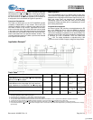
Single Clock Mode
The CY7C1303BV25 can be used with a single clock mode. In
this mode the device will recognize only the pair of input clocks
(K and K
) that control both the input and output registers. This
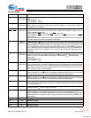
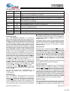
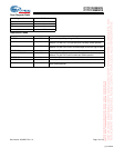
NC/36M N/A Address expansion for 36M. This pin is not connected to the die and so can be tied to any
voltage level on CY7C1303BV25/CY7C1306BV25.
GND/72M Input Address expansion for 72M. This pin has to be tied to GND on CY7C1303BV25.
NC/72M N/A Address expansion for 72M. This pin can be tied to any voltage level on CY7C1306BV25.
GND/144M Input Address expansion for 144M. This pin has to be tied to GND on
CY7C1303BV25/CY7C1306BV25.
GND/288M Input Address expansion for 288M. This pin has to be tied to GND on CY7C1306BV25.
NC N/A Not connected to the die. Can be tied to any voltage level.
V
REF
Input-
Reference
Reference Voltage Input. Static input used to set the reference level for HSTL inputs and Outputs
as well as AC measurement points.
V
DD
Power Supply Power supply inputs to the core of the device.
V
SS
Ground Ground for the device.
V
DDQ
Power Supply Power supply inputs for the outputs of the device.
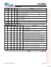
Pin Definitions (continued)
Name I/O Description
[+] Feedback


