CY7C1310AV18
CY7C1312AV18
CY7C1314AV18
PRELIMINARY
Document #: 38-05497 Rev. *A Page 6 of 21
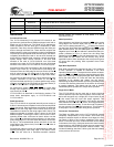
Introduction
Functional Overview
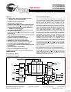
The CY7C1310AV18/CY7C1312AV18/CY7C1314AV18 are
synchronous pipelined Burst SRAMs equipped with both a
Read port and a Write port. The Read port is dedicated to
Read operations and the Write port is dedicated to Write
operations. Data flows into the SRAM through the Write port
and out through the Read Port. These devices multiplex the
address inputs in order to minimize the number of address pins
required. By having separate Read and Write ports, the QDR-II
completely eliminates the need to “turn-around” the data bus
and avoids any possible data contention, thereby simplifying
system design. Each access consists of two 8-bit data
transfers in the case of CY7C1310AV18, two 18-bit data
transfers in the case of CY7C1312AV18 and two 36-bit data
transfers in the case of CY7C1314AV18, in one clock cycles.
Accesses for both ports are initiated on the rising edge of the
positive Input Clock (K). All synchronous input timings are
referenced from the rising edge of the input clocks (K and K
)
and all output timings are referenced to the rising edge of
output clocks (C and C
or K and K when in single clock mode).
All synchronous data inputs (D
[x:0]
) inputs pass through input
registers controlled by the input clocks (K and K
). All
synchronous data outputs (Q
[x:0]
) outputs pass through output
registers controlled by the rising edge of the output clocks (C
and C
or K and K when in single clock mode).
All synchronous control (RPS
, WPS, BWS
[x:0]
) inputs pass
through input registers controlled by the rising edge of the
input clocks (K and K
).
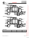
CY7C1312AV18 is described in the following sections. The
same basic descriptions apply to CY7C1310AV18 and
CY7C1314AV18.
Read Operations
The CY7C1312AV18 is organized internally as two arrays of
512Kx18. Accesses are completed in a burst of two sequential
18-bit data words. Read operations are initiated by asserting
RPS
active at the rising edge of the Positive Input Clock (K).
The address is latched on the rising edge of the K Clock. The
address presented to Address inputs is stored in the Read
address register. Following the next K clock rise the corre-
sponding lowest order 18-bit word of data is driven onto the
Q
[17:0]
using C as the output timing reference. On the subse-
quent rising edge of C, the next 18-bit data word is driven onto
the Q
[17:0]
. The requested data will be valid 0.45 ns from the
rising edge of the output clock (C and C
or K and K when in
single clock mode).
Synchronous internal circuitry will automatically tri-state the
outputs following the next rising edge of the Output Clocks
(C/C
). This will allow for a seamless transition between
devices without the insertion of wait states in a depth
expanded memory.
Write Operations
Write operations are initiated by asserting WPS
active at the
rising edge of the Positive Input Clock (K). On the same K
clock rise, the data presented to D
[17:0]
is latched and stored
into the lower 18-bit Write Data register provided BWS
[1:0]
are
both asserted active. On the subsequent rising edge of the
Negative Input Clock (K
), the address is latched and the infor-
mation presented to D
[17:0]
is stored into the Write Data
Register provided BWS
[1:0]
are both asserted active. The 36
bits of data are then written into the memory array at the
specified location. When deselected, the write port will ignore
all inputs after the pending Write operations have been
completed.
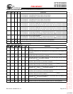
Byte Write Operations
Byte Write operations are supported by the CY7C1312AV18.
A write operation is initiated as described in the Write
Operation section above. The bytes that are written are deter-
mined by BWS
0
and BWS
1
which are sampled with each 18-bit
data word. Asserting the appropriate Byte Write Select input
during the data portion of a write will allow the data being
presented to be latched and written into the device.
Deasserting the Byte Write Select input during the data portion
of a write will allow the data stored in the device for that byte
to remain unaltered. This feature can be used to simplify
Read/Modify/Write operations to a Byte Write operation.
Single Clock Mode
The CY7C1312AV18 can be used with a single clock that
controls both the input and output registers. In this mode, the
device will recognize only a single pair of input clocks (K and
K
) that control both the input and output registers. This
operation is identical to the operation if the device had zero
skew between the K/K and C/C clocks. All timing parameters
remain the same in this mode. To use this mode of operation,
the user must tie C and C
HIGH at power on. This function is
a strap option and not alterable during device operation.
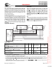
Concurrent Transactions
The Read and Write ports on the CY7C1312AV18 operate
completely independently of one another. Since each port
latches the address inputs on different clock edges, the user
can Read or Write to any location, regardless of the trans-
action on the other port. Also, reads and writes can be started
in the same clock cycle. If the ports access the same location
at the same time, the SRAM will deliver the most recent infor-
mation associated with the specified address location. This
includes forwarding data from a Write cycle that was initiated
on the previous K clock rise.
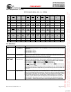
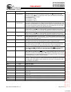
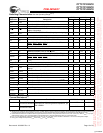
V
REF
Input-
Reference
Reference Voltage Input. Static input used to set the reference level for HSTL inputs
and Outputs as well as AC measurement points.
V
DD
Power Supply Power supply inputs to the core of the device.
V
SS
Ground Ground for the device.
V
DDQ
Power Supply Power supply inputs for the outputs of the device.
Pin Definitions (continued)
Pin Name I/O Pin Description
[+] Feedback


