CY7C1310AV18
CY7C1312AV18
CY7C1314AV18
PRELIMINARY
Document #: 38-05497 Rev. *A Page 18 of 21
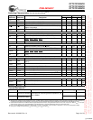
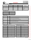
Identification Register Definitions
Instruction Field
CY7C1310AV18 CY7C1312AV18 CY7C1314AV18
Description2M x 8 1M x 18 512K x 36
Revision Number (31:29) 000 000 000 Version number.
Cypress Device ID (28:12) 11010011010000101 11010011010010101 11010011010100101 Defines the type of SRAM.
Cypress JEDEC ID (11:1) 00000110100 00000110100 00000110100 Allows unique identification of
SRAM vendor.
ID Register Presence (0) 1 1 1 Indicates the presence of an
ID register.
Scan Register Sizes
Register Name Bit Size
Instruction 3
Bypass 1
ID 32
Boundary Scan 107
Instruction Codes
Instruction Code Description
EXTEST 000 Captures the Input/Output ring contents.
IDCODE 001 Loads the ID register with the vendor ID code and places the register between TDI and TDO.
This operation does not affect SRAM operation.
SAMPLE Z 010 Captures the Input/Output contents. Places the boundary scan register between TDI and
TDO. Forces all SRAM output drivers to a High-Z state.
RESERVED 011 Do Not Use: This instruction is reserved for future use.
SAMPLE/PRELOAD 100 Captures the Input/Output ring contents. Places the boundary scan register between TDI and
TDO. Does not affect the SRAM operation.
RESERVED 101 Do Not Use: This instruction is reserved for future use.
RESERVED 110 Do Not Use: This instruction is reserved for future use.
BYPASS 111 Places the bypass register between TDI and TDO. This operation does not affect SRAM
operation.
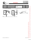
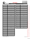
Boundary Scan Order
Bit # Bump ID
06R
16P
26N
37P
47N
57R
68R
78P
89R
911P
10 10P
11 10N
12 9P
13 10M
14 11N
15 9M
16 9N
17 11L
18 11M
19 9L
20 10L
21 11K
22 10K
23 9J
24 9K
25 10J
26 11J
27 11H
28 10G
29 9G
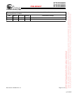
Boundary Scan Order (continued)
Bit # Bump ID
[+] Feedback


