CY7C1310BV18, CY7C1910BV18
CY7C1312BV18, CY7C1314BV18
Document #: 38-05619 Rev. *F Page 28 of 29
Document History Page
Document Title: CY7C1310BV18/CY7C1910BV18/CY7C1312BV18/CY7C1314BV18, 18-Mbit QDR™-II SRAM 2-Word Burst
Architecture
Document Number: 38-05619
Rev. ECN No.
Submission
Date
Orig, of
Change
Description of Change
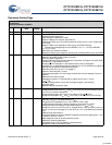
** 252474 See ECN SYT New datasheet
*A 325581 See ECN SYT Removed CY7C1910BV18 from the title
Included 300 MHz Speed Bin
Added Industrial Temperature Grade
Replaced TBDs for I
DD
and I
SB1
specifications
Replaced the TBDs on the Thermal Characteristics Table to Θ
JA
= 28.51°C/W and Θ
JC
= 5.91°C/W
Replaced TBDs in the Capacitance Table for the 165 FBGA Package
Changed the package diagram from BB165E (15 x 17 x 1.4 mm) to BB165D
(13 x 15 x 1.4 mm)
Added Pb-Free Product Information
Updated the Ordering Information by Shading and Unshading MPNs as per availability
*B 413997 See ECN NXR Converted from Preliminary to Final
Added CY7C1910BV18 part number to the title
Removed 300MHz Speed Bin
Changed address of Cypress Semiconductor Corporation on Page# 1 from “3901 North
First Street” to “198 Champion Court”
Changed C/C
Pin Description in the features section and Pin Description
Corrected Typo in Identification Register Definitions for CY7C1910BV18 on page# 16
Added power up sequence details and waveforms
Added foot notes #15, 16, and 17 on page# 18
Replaced Three state with Tri-state
Changed the description of I
X
from Input Load Current to Input Leakage Current on
page# 13
Modified the I
DD
and I
SB
values
Modified test condition in Footnote #20 on page# 19 from V
DDQ
< V
DD
to
V
DDQ
< V
DD
Replaced Package Name column with Package Diagram in the Ordering
Information table
Updated Ordering Information Table
*C 423334 See ECN NXR Changed the IEEE Standard # 1149.1-1900 to 1149.1-2001
Changed the Minimum Value of t
SC
and t
HC
from 0.5ns to 0.35ns for 250 MHz and 0.6
ns to 0.4 ns for 200 MHz speed bins
Changed the description of t
SA
from K Clock Rise to Clock (K/K) Rise
Changed the description of t
SC
and
t
HC
from Clock (K and K) Rise to K Clock Rise
*D 472384 See ECN NXR Modified the ZQ Definition from Alternately, this pin is connected directly to V
DD
to
Alternately, this pin is connected directly to V
DDQ
Changed the IEEE Standard # from 1149.1-2001 to 1149.1-1900
Included Maximum Ratings for Supply Voltage on V
DDQ
Relative to GND
Changed the Maximum Ratings for DC Input Voltage from V
DDQ
to V
DD
Changed t
TH
and t
TL
from 40 ns to 20 ns, changed t
TMSS
, t
TDIS
, t
CS
, t
TMSH
, t
TDIH
, t
CH
from
10 ns to 5 ns and changed t
TDOV
from 20 ns to 10 ns in Tap Switching Character-
istics.
Modified Power Up waveform
Changed the Maximum rating of Ambient Temperature with Power Applied from –10°C
to +85°C to –55°C to +125°C
Added additional notes in the AC parameter section
Modified AC Switching Waveform
Corrected the typo In the Tap Switching Characteristics.
Updated the Ordering Information Table
[+] Feedback


