CY7C1318CV18
CY7C1320CV18
Document Number: 001-07160 Rev. *F Page 25 of 26
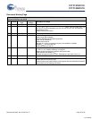
Document History Page
Document Title: CY7C1318CV18/CY7C1320CV18, 18-Mbit DDR II SRAM 2-Word Burst Architecture
Document Number: 001-07160
Rev. ECN No.
Submission
Date
Orig. of
Change
Description of Change
** 433284 See ECN NXR New data sheet
*A 462615 See ECN NXR Changed t
TH
and t
TL
from 40 ns to 20 ns, changed t
TMSS
, t
TDIS
, t
CS
, t
TMSH
, t
TDIH
, t
CH
from
10 ns to 5 ns and changed t
TDOV
from 20 ns to 10 ns in TAP AC Switching
Characteristics table
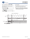
Modified Power-Up waveform
*B 503690 See ECN VKN Minor change: Moved data sheet to web
*C 1523383 See ECN VKN/AESA Converted from preliminary to final
Updated Logic Block diagram
Removed 300 MHz and 278 MHz speed bins
Added 267 MHz speed bin
Updated I
DD
/I
SB
specs
Changed DLL minimum operating frequency from 80MHz to 120MHz
Changed t
CYC
max spec to 8.4ns
Modified footnotes 20 and 28
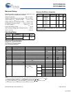
*D 2507747 See ECN VKN/PYRS Changed Ambient Temperature with Power Applied from “–10°C to +85°C” to “–55°C
to +125°C” in the “Maximum Ratings“ on page 20
Updated power up sequence waveform and its description
Added footnote #19 related to I
DD
Changed Θ
JA
spec from 28.51 to 18.7; Changed Θ
JC
spec from 5.91 to 4.5
*E 2518624 See ECN NXR/PYRS Changed JTAG ID (31:29) from 001 to 000
*F 2755838 08/25/2009 VKN/AESA Removed x8 and x9 part number details
Included Soft Error Immunity Data
Modified Ordering Information table by including parts that are available and modified
the disclaimer for the Ordering information.
[+] Feedback


