PRELIMINARY
CY7C1330AV25
CY7C1332AV25
Document No: 001-07844 Rev. *A Page 11 of 19
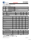
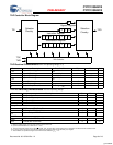
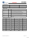
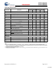
Scan Register Sizes
Register Name Bit Size—CY7C1330AV25 Bit Size—CY7C1332AV25
Instruction 3 3
Bypass 1 1
ID 32 32
Boundary Scan 70 51
Instruction Codes
Instruction Code Description
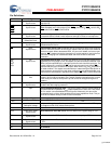
EXTEST 000 Captures the Input/Output ring contents.
IDCODE 001 Loads the ID register with the vendor ID code and places the register between TDI
and TDO. This operation does not affect SRAM operation.
SAMPLE Z 010 Captures the Input/Output contents. Places the boundary scan register between
TDI and TDO. Forces all SRAM output drivers to a High-Z state.
RESERVED 011 Do Not Use: This instruction is reserved for future use.
SAMPLE/PRELOAD 100 Captures the Input/Output ring contents. Places the boundary scan register
between TDI and TDO. Does not affect the SRAM operation.
RESERVED 101 Do Not Use: This instruction is reserved for future use.
RESERVED 110 Do Not Use: This instruction is reserved for future use.
BYPASS 111 Places the bypass register between TDI and TDO. This operation does not affect
SRAM operation.
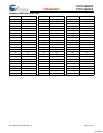
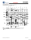
Boundary Scan Order (1 Mbit x 18)
Bit # Bump ID Bit # Bump ID Bit # Bump ID
15R 187E 351H
26T 196D 363G
34P 206A 374D
46R 216C 384E
55T 225C 394G
67T 235A 404H
77P 246B 414M
86N 255B 422K
96L 263B 431L
10 7K 27 2B 44 2M
11 5L 28 3A 45 1N
12 4L 29 3C 46 2P
13 4K 30 2C 47 3T
14 4F 31 2A 48 2R
15 6H 32 1D 49 4N
16 7G 33 2E 50 2T
17 6F 34 2G 51 3R
[+] Feedback


