CY7C1352G
Document #: 38-05514 Rev. *D Page 12 of 12
Document History Page
Document Title: CY7C1352G 4-Mbit (256K x 18) Pipelined SRAM with NoBL™ Architecture
Document Number: 38-05514
REV. ECN NO.
Issue
Date
Orig. of
Change Description of Change
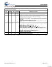
** 224362 See ECN RKF New data sheet
*A 288431 See ECN VBL Deleted 100 MHz and 225 MHz
Changed TQFP package in Ordering Information section to lead-free TQFP
*B 332895 See ECN SYT Modified Address Expansion balls in the pinouts for 100 TQFP Package as per
JEDEC standards and updated the Pin Definitions accordingly
Modified V
OL,
V
OH
test conditions
Replaced TBD’s for Θ
JA
and Θ
JC
to their respective values on the Thermal Resis-
tance table
Added lead-free product information for 119 BGA
Updated the Ordering Information by shading and unshading MPNs as per avail-
ability
*C 419256 See ECN RXU Converted from Preliminary to Final
Changed address of Cypress Semiconductor Corporation on Page# 1 from “3901
North First Street” to “198 Champion Court”
Modified test condition from V
IH
< V
DD
to
V
IH
< V
DD
Modified test condition from V
DDQ
< V
DD
to V
DDQ
< V
DD
Modified “Input Load” to “Input Leakage Current except ZZ and MODE” in the
Electrical Characteristics Table
Replaced Package Name column with Package Diagram in the Ordering Information
table
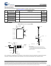
Replaced Package Diagram of 51-85050 from *A to *B
Updated the Ordering Information
*D 480124 See ECN VKN Added the Maximum Rating for Supply Voltage on V
DDQ
Relative to GND.
Updated the Ordering Information table.
[+] Feedback


