CY7C1380D, CY7C1382D
CY7C1380F, CY7C1382F
Document #: 38-05543 Rev. *F Page 7 of 34
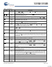
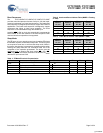
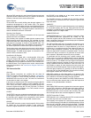
MODE Input-Static Selects burst order. When tied to GND selects linear burst sequence. When tied to V
DD
or left
floating selects interleaved burst sequence. This is a strap pin and must remain static during
device operation. Mode pin has an internal pull up.
TDO JTAG serial
output
Synchronous
Serial data-out to the JTAG circuit. Delivers data on the negative edge of TCK. If the JTAG
feature is not being utilized, this pin must be disconnected. This pin is not available on TQFP
packages.
TDI JTAG serial
input
Synchronous
Serial data-in to the JTAG circuit. Sampled on the rising edge of TCK. If the JTAG feature is
not being utilized, this pin can be disconnected or connected to V
DD
. This pin is not available on
TQFP packages.
TMS JTAG serial
input
Synchronous
Serial data-in to the JTAG circuit. Sampled on the rising edge of TCK. If the JTAG feature is
not being utilized, this pin can be disconnected or connected to V
DD
. This pin is not available on
TQFP packages.
TCK JTAG-
Clock
Clock input to the JTAG circuitry. If the JTAG feature is not being utilized, this pin must be
connected to V
SS
. This pin is not available on TQFP packages.
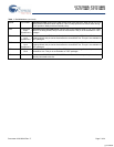
NC – No Connects. 36M, 72M, 144M, 288M, 576M, and 1G are address expansion pins and are not
internally connected to the die.
Table 1. Pin Definitions (continued)
[+] Feedback


