CY7C1380DV25, CY7C1380FV25
CY7C1382DV25, CY7C1382FV25
Document #: 38-05546 Rev. *E Page 13 of 29
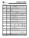
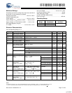
instruction. When HIGH, it will enable the output buffers to
drive the output bus. When LOW, this bit will place the output
bus into a High-Z condition.
This bit can be set by entering the SAMPLE/PRELOAD or
EXTEST command, and then shifting the desired bit into that
cell, during the Shift-DR state. During Update-DR, the value
loaded into that shift-register cell will latch into the preload
register. When the EXTEST instruction is entered, this bit will
directly control the output Q-bus pins. Note that this bit is
preset HIGH to enable the output when the device is powered
up, and also when the TAP controller is in the Test-Logic-Reset
state.
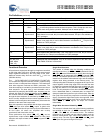
Reserved
These instructions are not implemented but are reserved for
future use. Do not use these instructions.
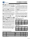
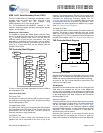
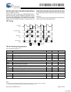
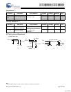
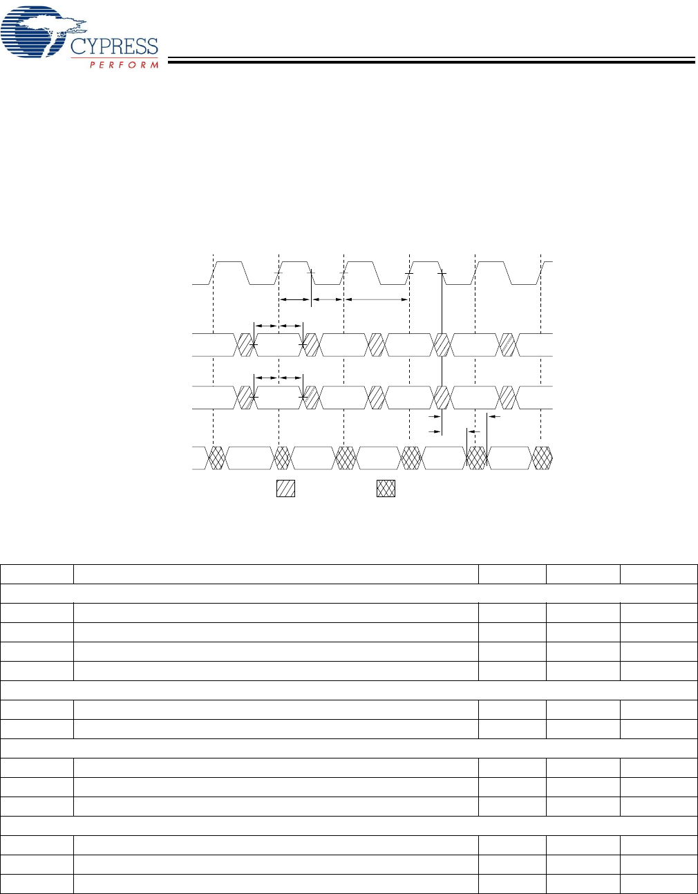
TAP Timing
TAP AC Switching Characteristics
Over the Operating Range
[10, 11]
Parameter Description Min. Max. Unit
Clock
t
TCYC
TCK Clock Cycle Time 50 ns
t
TF
TCK Clock Frequency 20 MHz
t
TH
TCK Clock HIGH time 20 ns
t
TL
TCK Clock LOW time 20 ns
Output Times
t
TDOV
TCK Clock LOW to TDO Valid 10 ns
t
TDOX
TCK Clock LOW to TDO Invalid 0 ns
Setup Times
t
TMSS
TMS Setup to TCK Clock Rise 5 ns
t
TDIS
TDI Setup to TCK Clock Rise 5 ns
t
CS
Capture Setup to TCK Rise 5 ns
Hold Times
t
TMSH
TMS Hold after TCK Clock Rise 5 ns
t
TDIH
TDI Hold after Clock Rise 5 ns
t
CH
Capture Hold after Clock Rise 5 ns
t
TL
Test Clock
(TCK)
123456
Test Mode Select
(TMS)
t
TH
Test Data-Out
(TDO)
t
CYC
Test Data-In
(TDI)
t
TMSH
t
TMSS
t
TDIH
t
TDIS
t
TDOX
t
TDOV
DON’T CARE UNDEFINED
Notes:
10.t
CS
and t
CH
refer to the setup and hold time requirements of latching data from the boundary scan register.
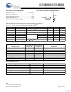
11.Test conditions are specified using the load in TAP AC test conditions. t
R
/t
F
= 1ns.
[+] Feedback


