CY7C1410AV18, CY7C1425AV18
CY7C1412AV18, CY7C1414AV18
Document #: 38-05615 Rev. *E Page 28 of 29
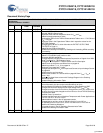
Document History Page
Document Title: CY7C1410AV18/CY7C1425AV18/CY7C1412AV18/CY7C1414AV18, 36-Mbit QDR™-II SRAM 2-Word Burst
Architecture
Document Number: 38-05615
REV. ECN NO.
SUBMISSION
DATE
ORIG. OF
CHANGE
DESCRIPTION OF CHANGE
** 247331 See ECN SYT New Data Sheet
*A 326519 See ECN SYT Removed CY7C1425AV18 from the title
Included 300 MHz Speed grade
Replaced TBDs with their respective values for I
DD
and I
SB1
Added Industrial temperature grade
Replaced the TBDs on the Thermal Characteristics Table to Θ
JA
= 17.2°C/W and
Θ
JC
= 3.2°C/W
Replaced TBDs in the Capacitance Table to their respective values for the
165 FBGA Package
Changed typo of bit # 47 to bit # 108 under the EXTEST OUTPUT BUS
TRI-STATE on Page 16
Added Pb-free Product Information
Updated the Ordering Information by Shading and Unshading MPNs according
to availability
*B 413953 See ECN NXR Converted from preliminary to final.
Added CY7C1425AV18 part number to title.
Removed 300-MHz speed Bin.
Changed address of Cypress Semiconductor Corporation on Page# 1 from “3901
North First Street” to “198 Champion Court”
Changed C, C
Description in Feature Section and Pin Description.
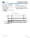
Added Power up sequence and Wave form on page# 19
Added foot notes # 13, 14, 15 on page# 19
Replaced Three-state with Tri-state.
Changed the description of I
X
from Input Load Current to Input Leakage Current
on page# 20
Modified the I
DD
and I
SB
values.
Modified test condition in Footnote # 20 on page# 20 from V
DDQ
< V
DD
to
V
DDQ
< V
DD.
Replaced Package Name column with Package Diagram in the Ordering
Information table.
Updated Ordering Information Table.
*C 468029 See ECN NXR Modified the ZQ Definition from Alternately, this pin can be connected directly to
V
DD
to Alternately, this pin can be connected directly to V
DDQ.
Included Maximum Ratings for Supply Voltage on V
DDQ
Relative to GND
Changed the Maximum Ratings for DC Input Voltage from V
DDQ
to V
DD.
Changed t
TH
and t
TL
from 40 ns to 20 ns, changed t
TMSS
, t
TDIS
, t
CS
, t
TMSH
, t
TDIH
,
t
CH
from
10 ns to 5 ns and changed t
TDOV
from 20 ns to 10 ns in TAP AC Switching
Characteristics table
Modified Power Up waveform
Changed the Maximum rating of Ambient Temperature with Power Applied from
–10°C to +85°C to –55°C to +125°C
Added additional notes in the AC parameter section
Changed the t
SC
and t
HC
value for 250 MHz from 0.5 ns to 0.35 ns,
for 200 MHz from 0.6 ns to 0.4 ns, and for 167 MHz from 0.7 ns to 0.5 ns.
Modified AC Switching Waveform.
Corrected the typo In the AC Switching Characteristics Table.
Updated the Ordering Information Table.
*D 1274725 See ECN VKN/AESA Modified footnote# 30
[+] Feedback


