CY7C1441AV33
CY7C1443AV33,CY7C1447AV33
Document #: 38-05357 Rev. *G Page 30 of 31
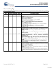
Document History Page
Document Title: CY7C1441AV33/CY7C1443AV33/CY7C1447AV33 36-Mbit (1M x 36/2M x 18/512K x 72) Flow-Through SRAM
Document Number: 38-05357
REV. ECN NO. Issue Date
Orig. of
Change Description of Change
** 124459 03/06/03 CJM New Data Sheet
*A 254910 See ECN SYT Part number changed from previous revision. New and old part number differ by
the letter “A”
Modified Functional Block diagrams
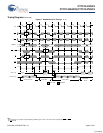
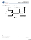
Modified switching waveforms
Added Footnote #13 (32-Bit Vendor I.D Code changed)
Added Boundary scan information
Added I
DD
, I
X
and I
SB
values in the DC Electrical Characteristics
Added t
POWER
specifications in Switching Characteristics table
Removed 119 PBGA Package
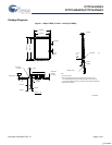
Changed 165 FBGA Package from BB165C (15 x 17 x 1.20 mm) to BB165
(15 x 17 x 1.40 mm)
Changed 209-Lead PBGA BG209 (14 x 22 x 2.20 mm) to BB209A
(14 x 22 x 1.76 mm)
*B 300131 See ECN SYT Removed 150 and 117 MHz Speed Bins
Changed
Θ
JA
and Θ
JC
from TBD to 25.21 and 2.58 °C/W respectively for TQFP
Package on Pg # 21
Added lead-free information for 100-pin TQFP, 165 FBGA and 209 BGA
Packages.
Added comment of ‘Lead-free BG and BZ packages availability’ below the
Ordering Information
*C 320813 See ECN SYT Changed H9 pin from V
SSQ
to V
SS
on the Pin Configuration table for 209 FBGA
Changed the test condition from V
DD
= Min. to V
DD
= Max for V
OL
in the Electrical
Characteristics table.
Replaced the TBD’s for I
DD
, I
SB1
, I
SB2
, I
SB3
and I
SB4
to their respective values.
Replaced TBD’s for Θ
JA
and Θ
JC
to their respective values for 165 fBGA and 209
fBGA packages on the Thermal Resistance table.
Changed C
IN
,C
CLK
and C
IO
to 6.5, 3 and 5.5 pF from 5, 5 and 7 pF for TQFP
Package.
Removed “Lead-free BG and BZ packages availability” comment below the
Ordering Information
*D 331551 See ECN SYT Modified Address Expansion balls in the pinouts for 165 FBGA and 209 BGA
Packages as per JEDEC standards and updated the Pin Definitions accordingly
Modified V
OL,
V
OH
test conditions
Replaced TBD to 100 mA for I
DDZZ
Changed C
IN
, C
CLK
and C
IO
to 7, 7and 6 pF from 5, 5 and 7 pF for 165 FBGA
Package.
Added Industrial Temperature Grade
Changed I
SB2
and I
SB4
from 100 and 110 mA to 120 and 135 mA respectively
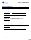
Updated the Ordering Information by shading and unshading MPNs as per avail-
ability
[+] Feedback


