CY7C1471V33
CY7C1473V33
CY7C1475V33
Document #: 38-05288 Rev. *J Page 32 of 32
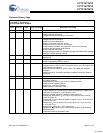
*I 472335 See ECN VKN Corrected the typo in the pin configuration for 209-Ball FBGA pinout
(Corrected the ball name for H9 to V
SS
from V
SSQ
).
Added the Maximum Rating for Supply Voltage on V
DDQ
Relative to GND.
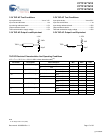
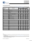
Changed t
TH
, t
TL
from 25 ns to 20 ns and t
TDOV
from 5 ns to 10 ns in TAP AC
Switching Characteristics table.
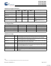
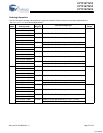
Updated the Ordering Information table.
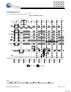
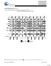
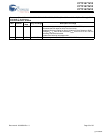
*J 1274732 See ECN VKN/AESA Corrected typo in the “NOP, STALL and DESELECT Cycles” waveform
Document Title: CY7C1471V33/CY7C1473V33/CY7C1475V33, 72-Mbit (2M x 36/4M x 18/1M x 72) Flow-Through SRAM
with NoBL™ Architecture
Document Number: 38-05288
REV. ECN NO.
Issue
Date
Orig. of Change Description of Change
[+] Feedback


