CY7C1471BV25
CY7C1473BV25, CY7C1475BV25
Document #: 001-15013 Rev. *E Page 21 of 30
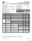
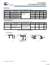
Capacitance
Tested initially and after any design or process change that may affect these parameters.
Parameter Description Test Conditions
100 TQFP
Max
165 FBGA
Max
209 FBGA
Max
Unit
C
ADDRESS
Address Input Capacitance T
A
= 25°C, f = 1 MHz,
V
DD
= 2.5V
V
DDQ
= 2.5V
6 6 6 pF
C
DATA
Data Input Capacitance 5 5 5 pF
C
CTRL
Control Input Capacitance 8 8 8 pF
C
CLK
Clock Input Capacitance 6 6 6 pF
C
IO
Input-Output Capacitance 5 5 5 pF
Thermal Resistance
Tested initially and after any design or process change that may affect these parameters.
Parameter Description Test Conditions
100 TQFP
Package
165 FBGA
Package
209 FBGA
Package
Unit
Θ
JA
Thermal Resistance
(Junction to Ambient)
Test conditions follow
standard test methods and
procedures for measuring
thermal impedance,
according to EIA/JESD51.
24.63 16.3 15.2 °C/W
Θ
JC
Thermal Resistance
(Junction to Case)
2.28 2.1 1.7 °C/W
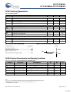
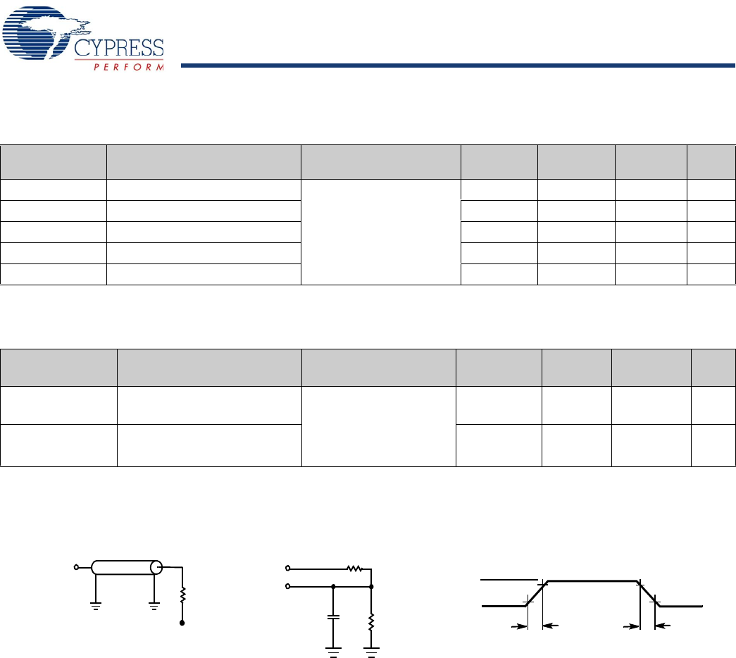
Figure 7. AC Test Loads and Waveforms
OUTPUT
R = 1667Ω
R = 1538Ω
5pF
INCLUDING
JIG AND
SCOPE
(a)
(b)
OUTPUT
R
L
= 50Ω
Z
0
= 50Ω
V
L
= 1.25V
2.5V
ALL INPUT PULSES
V
DDQ
GND
90%
10%
90%
10%
≤ 1 ns
≤ 1 ns
(c)
2.5V IO Test Load
[+] Feedback


