CY7C1480V25
CY7C1482V25
CY7C1486V25
Document #: 38-05282 Rev. *H Page 16 of 32
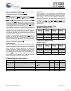
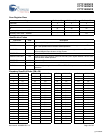
Scan Register Sizes
Register Name Bit Size (x36) Bit Size (x18) Bit Size (x72)
Instruction 3 3 3
Bypass 1 1 1
ID 32 32 32
Boundary Scan Order – 165FBGA 73 54 -
Boundary Scan Order – 209BGA - - 112
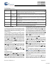
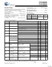
Identification Codes
Instruction Code Description
EXTEST 000 Captures the IO ring contents.
IDCODE 001 Loads the ID register with the vendor ID code and places the register between TDI and
TDO. This operation does not affect SRAM operations.
SAMPLE Z 010 Captures the IO ring contents. Places the boundary scan register between TDI and TDO.
Forces all SRAM output drivers to a High-Z state.
RESERVED 011 Do Not Use: This instruction is reserved for future use.
SAMPLE/PRELOAD 100 Captures the IO ring contents. Places the boundary scan register between TDI and TDO.
Does not affect SRAM operation.
RESERVED 101 Do Not Use: This instruction is reserved for future use.
RESERVED 110 Do Not Use: This instruction is reserved for future use.
BYPASS 111 Places the bypass register between TDI and TDO. This operation does not affect SRAM
operations.
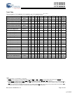
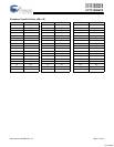
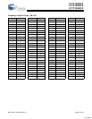
Boundary Scan Exit Order (2M x 36)
Bit # 165-Ball ID Bit # 165-Ball ID Bit # 165-Ball ID Bit # 165-Ball ID
1 C1 21 R3 41 L10 61 B8
2D1 22 P2 42K11 62 A7
3E1 23 R4 43J11 63 B7
4D2 24 P6 44K10 64 B6
5 E2 25 R6 45 J10 65 A6
6F1 26 N6 46H11 66B5
7G1 27P11 47G11 67 A5
8F2 28 R8 48F11 68A4
9G2 29 P3 49E11 69 B4
10 J1 30 P4 50 D10 70 B3
11 K1 31 P8 51 D11 71 A3
12 L1 32 P9 52 C11 72 A2
13 J2 33 P10 53 G10 73 B2
14 M1 34 R9 54 F10
15 N1 35 R10 55 E10
16 K2 36 R11 56 A10
17 L2 37 N11 57 B10
18 M2 38 M11 58 A9
19 R1 39 L11 59 B9
20 R2 40 M10 60 A8
[+] Feedback


