CY7C1511V18, CY7C1526V18
CY7C1513V18, CY7C1515V18
Document Number: 38-05363 Rev. *F Page 31 of 32
Document History Page
Document Title: CY7C1511V18/CY7C1526V18/CY7C1513V18/CY7C1515V18, 72-Mbit QDR™-II SRAM 4-Word Burst Archi-
tecture
Document Number: 38-05363
REV. ECN NO.
SUBMISSION
DATE
ORIG. OF
CHANGE
DESCRIPTION OF CHANGE
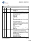
** 226981 See ECN DIM New Data Sheet
*A 257089 See ECN NJY Modified JTAG ID code for x9 option in the ID register definition on page 20 of
the data sheet
Included thermal values
Modified capacitance values table: included capacitance values for x8, x18
and x36 options
*B 319496 See ECN SYT Removed CY7C1526V18 from the title
Included 300-MHz Speed Bin
Added footnote #1 and accordingly edited the V
SS
/144M And V
SS
/288M on
the Pin Definitions table
Added Industrial temperature grade
Replaced TBDs for I
DD
and I
SB1
for 300 MHz, 250 MHz, 200 MHz and 167
MHz speed grades
Changed the C
IN
from 5 pF to 5.5 pF and C
O
from 7 pF to 8 pF in the
Capacitance Table
Changed typo of bit # 47 to bit # 108 under the EXTEST OUTPUT BUS
TRI-STATE on Page 17
Removed the capacitance value column for the x9 option from Capacitance
Table
Added lead-free product information
Updated the Ordering Information by Shading and unshading as per avail-
ability
*C 403231 See ECN NXR Converted from Preliminary to Final
Added CY7C1526V18 part number to the title
Added 278-MHz speed Bin
Changed address of Cypress Semiconductor Corporation on Page# 1 from
“3901 North First Street” to “198 Champion Court”
Changed C/C
Pin Description in the features section and Pin Description
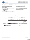
Added power-up sequence details and waveforms
Added foot notes #16, 17, 18 on page# 19
Changed the description of I
X
from Input Load Current to Input Leakage
Current
on page# 20
Modified the I
DD
and I
SB
values
Modified test condition in Footnote #19 on page # 20 from V
DDQ
< V
DD
to
V
DDQ
< V
DD
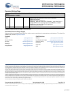
Replaced Package Name column with Package Diagram in the Ordering
Information table
Updated Ordering Information Table
*D 467290 See ECN NXR Modified the ZQ Definition from Alternately, this pin can be connected directly
to V
DD
to Alternately, this pin can be connected directly to V
DDQ
Included Maximum Ratings for Supply Voltage on V
DDQ
Relative to GND
Changed the Maximum Ratings for DC Input Voltage from V
DDQ
to V
DD
Changed t
TCYC
from 100 ns to 50 ns, changed t
TH
and t
TL
from 40 ns to 20 ns,
changed t
TMSS
, t
TDIS
, t
CS
, t
TMSH
, t
TDIH
, t
CH
from
10 ns to 5 ns and changed
t
TDOV
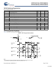
from 20 ns to 10 ns in TAP AC Switching Characteristics table
Modified Power-Up waveform
Changed the Maximum rating of Ambient Temperature with Power Applied
from –10°C to +85°C to –55°C to +125°C
Added additional notes in the AC parameter section
Modified AC Switching Waveform
Updated the Typo in the AC Switching Characteristics Table
Updated the Ordering Information Table
[+] Feedback


