PRELIMINARY
CY7C2561KV18, CY7C2576KV18
CY7C2563KV18, CY7C2565KV18
Document Number: 001-15887 Rev. *E Page 6 of 29
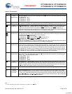
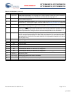
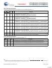
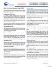
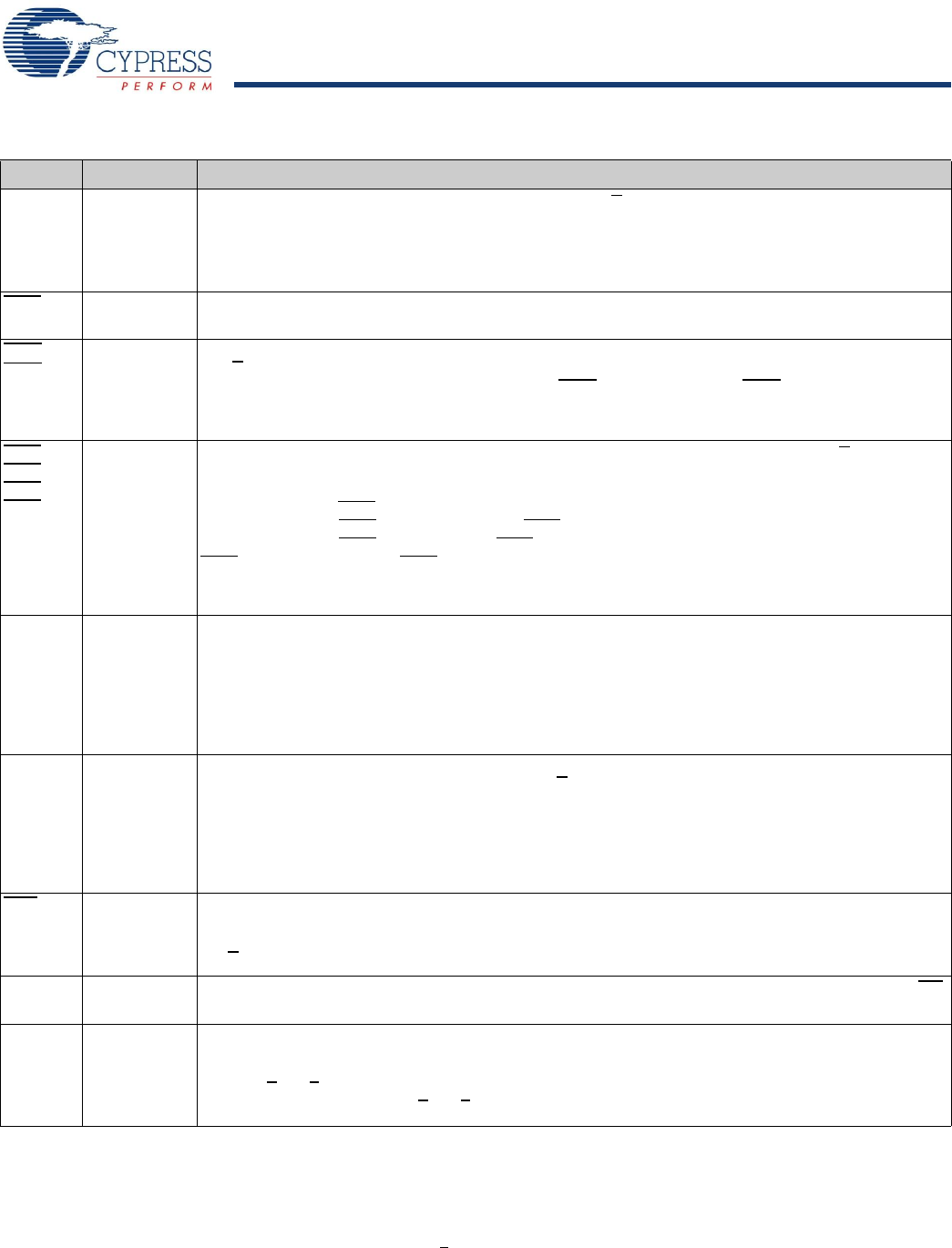
Table 2. Pin Definitions
Pin Name IO Pin Description
D
[x:0]
Input-
Synchronous
Data Input Signals. Sampled on the rising edge of K and K clocks when valid write operations are active.
CY7C2561KV18 − D
[7:0]
CY7C2576KV18 − D
[8:0]
CY7C2563KV18 − D
[17:0]
CY7C2565KV18 − D
[35:0]
WPS Input-
Synchronous
Write Port Select − Active LOW. Sampled on the rising edge of the K clock. When asserted active, a
write operation is initiated. Deasserting deselects the write port. Deselecting the write port ignores D
[x:0]
.
NWS
0
,
NWS
1
,
Input-
Synchronous
Nibble Write Select 0, 1 − Active LOW (CY7C2561KV18 Only). Sampled on the rising edge of the K
and K
clocks
when write operations are active
. Used to select which nibble is written into the device
during the current portion of the write operations.
NWS
0
controls D
[3:0]
and NWS
1
controls D
[7:4]
.
All the Nibble Write Selects are sampled on the same edge as the data. Deselecting a Nibble Write Select
ignores the corresponding nibble of data and it is not written into the device
.
BWS
0
,
BWS
1
,
BWS
2
,
BWS
3
Input-
Synchronous
Byte Write Select 0, 1, 2 and 3 − Active LOW. Sampled on the rising edge of the K and K clocks when
write operations are active. Used to select which byte is written into the device during the current portion
of the write operations. Bytes not written remain unaltered.
CY7C2576KV18 − BWS
0
controls D
[8:0]
CY7C2563KV18 − BWS
0
controls D
[8:0]
and BWS
1
controls D
[17:9].
CY7C2565KV18 − BWS
0
controls D
[8:0]
, BWS
1
controls D
[17:9]
,
BWS
2
controls D
[26:18]
and BWS
3
controls D
[35:27].
All the Byte Write Selects are sampled on the same edge as the data. Deselecting a Byte Write Select
ignores the corresponding byte of data and it is not written into the device
.
A Input-
Synchronous
Address Inputs. Sampled on the rising edge of the K clock during active read and write operations. These
address inputs are multiplexed for both read and write operations. Internally, the device is organized as
8M x 8 (4 arrays each of 2M x 8) for CY7C2561KV18, 8M x 9 (4 arrays each of 2M x 9) for CY7C2576KV18,
4M x 18 (4 arrays each of 1M x 18) for CY7C2563KV18 and 2M x 36 (4 arrays each of 512K x 36) for
CY7C2565KV18. Therefore, only 21 address inputs are needed to access the entire memory array of
CY7C2561KV18 and CY7C2576KV18, 20 address inputs for CY7C2563KV18 and 19 address inputs for
CY7C2565KV18. These inputs are ignored when the appropriate port is deselected.
Q
[x:0]
Outputs-
Synchronous
Data Output Signals. These pins drive out the requested data when the read operation is active. Valid
data is driven out on the rising edge of the K and K
clocks during read operations. On deselecting the
read port, Q
[x:0]
are automatically tri-stated.
CY7C2561KV18 − Q
[7:0]
CY7C2576KV18 − Q
[8:0]
CY7C2563KV18 − Q
[17:0]
CY7C2565KV18 − Q
[35:0]
RPS Input-
Synchronous
Read Port Select − Active LOW. Sampled on the rising edge of positive input clock (K). When active, a
read operation is initiated. Deasserting deselects the read port. When deselected, the pending access is
allowed to complete and the output drivers are automatically tri-stated following the next rising edge of
the K
clock. Each read access consists of a burst of four sequential transfers.
QVLD Valid output
indicator
Valid Output Indicator. The Q Valid indicates valid output data. QVLD is edge aligned with CQ and CQ
.
ODT
[3]
On-Die
Termination
input pin
On-Die Termination Input. This pin is used for On-Die termination of the input signals. ODT range
selection is made during power up initialization. A LOW on this pin selects a low range that follows RQ/3.33
for 175Ω <
RQ < 350Ω (where RQ is the resistor tied to ZQ pin). A HIGH on this pin selects a high range
that follows RQ/1.66 for 175Ω <
RQ < 250Ω (where RQ is the resistor tied to ZQ pin). When left floating,
a high range termination value is selected by default.
Note
3. On-Die Termination (ODT) feature is supported for D
[x:0]
, BWS
[x:0]
, and K/K inputs.
[+] Feedback


