CY7C68013A, CY7C68014A
CY7C68015A, CY7C68016A
Document #: 38-08032 Rev. *L Page 11 of 62
3.12.5 Default Full-Speed Alternate Settings
3.12.6 Default High-Speed Alternate Settings
3.13 External FIFO Interface
3.13.1 Architecture
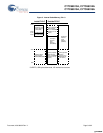
The FX2LP slave FIFO architecture has eight 512 byte blocks in
the endpoint RAM that directly serve as FIFO memories and are
controlled by FIFO control signals (such as IFCLK, SLCS#,
SLRD, SLWR, SLOE, PKTEND, and flags).
In operation, some of the eight RAM blocks fill or empty from the
SIE, while the others are connected to the IO transfer logic. The
transfer logic takes two forms, the GPIF for internally generated
control signals and the slave FIFO interface for externally
controlled transfers.
3.13.2 Master/Slave Control Signals
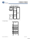
The FX2LP endpoint FIFOS are implemented as eight physically
distinct 256x16 RAM blocks. The 8051/SIE can switch any of the
RAM blocks between two domains, the USB (SIE) domain and
the 8051-IO Unit domain. This switching is done virtually instan-
taneously, giving essentially zero transfer time between “USB
FIFOS” and “Slave FIFOS.” Because they are physically the
same memory no bytes are actually transferred between buffers.
At any given time, some RAM blocks are filling/emptying with
USB data under SIE control, while other RAM blocks are
available to the 8051, the IO control unit or both. The RAM blocks
operate as single port in the USB domain, and dual port in the
8051-IO domain. The blocks can be configured as single,
double, triple, or quad buffered as previously shown.
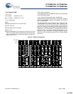
The IO control unit implements either an internal master (M for
master) or external master (S for Slave) interface.
In Master (M) mode, the GPIF internally controls FIFOADR[1..0]
to select a FIFO. The RDY pins (two in the 56-pin package, six
in the 100-pin and 128-pin packages) can be used as flag inputs
from an external FIFO or other logic if desired. The GPIF can be
run from either an internally derived clock or externally supplied
clock (IFCLK), at a rate that transfers data up to 96 Megabytes/s
(48-MHz IFCLK with 16-bit interface).
In Slave (S) mode, the FX2LP accepts either an internally
derived clock or externally supplied clock (IFCLK, max frequency
48 MHz) and SLCS#, SLRD, SLWR, SLOE, PKTEND signals
from external logic. When using an external IFCLK, the external
clock must be present before switching to the external clock with
the IFCLKSRC bit. Each endpoint can individually be selected
for byte or word operation by an internal configuration bit and a
Slave FIFO Output Enable signal SLOE enables data of the
selected width. External logic must ensure that the output enable
signal is inactive when writing data to a slave FIFO. The slave
interface can also operate asynchronously, where the SLRD and
SLWR signals act directly as strobes, rather than a clock qualifier
as in synchronous mode. The signals SLRD, SLWR, SLOE and
PKTEND are gated by the signal SLCS#.
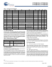
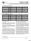
Table 6. Default Full-Speed Alternate Settings
[4, 5]
Alternate Setting 0 1 2 3
ep0 64 64 64 64
ep1out 0 64 bulk 64 int 64 int
ep1in 0 64 bulk 64 int 64 int
ep2 0 64 bulk out (2×) 64 int out (2×) 64 iso out (2×)
ep4 0 64 bulk out (2×) 64 bulk out (2×) 64 bulk out (2×)
ep6 0 64 bulk in (2×) 64 int in (2×) 64 iso in (2×)
ep8 0 64 bulk in (2×) 64 bulk in (2×) 64 bulk in (2×)
Notes
4. “0” means “not implemented.”
5. “2×” means “double buffered.”
6. Even though these buffers are 64 bytes, they are reported as 512 for USB 2.0 compliance. The user must never transfer packets larger than 64 bytes to EP1.
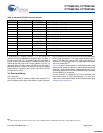
Table 7. Default High-Speed Alternate Settings
[4, 5]
Alternate Setting 0 1 2 3
ep0 64 64 64 64
ep1out 0 512 bulk
[6]
64 int 64 int
ep1in 0 512 bulk
[6]
64 int 64 int
ep2 0 512 bulk out (2×) 512 int out (2×) 512 iso out (2×)
ep4 0 512 bulk out (2×) 512 bulk out (2×) 512 bulk out (2×)
ep6 0 512 bulk in (2×) 512 int in (2×) 512 iso in (2×)
ep8 0 512 bulk in (2×) 512 bulk in (2×) 512 bulk in (2×)
[+] Feedback [+] Feedback


