November 7, 2008
Errata Document for PSoC
®
CY8C20x46, CY8C20x66
CY8C20x46, CY8C20x66
Cypress Semiconductor Corporation • 198 Champion Court • San Jose, CA 95134 • 408.943.2600
November 7, 2008 Document No. 001-32940 Rev. *C 1
This document describes the errata for the PSoC
®
CY8C20x46 and CY8C20x66. Details include errata trigger
conditions, scope of impact, available workarounds, and silicon revision applicability. Compare this document to the
device’s data sheet for a complete functional description. This document is not available on the external Cypress
web site.
Contact your local Cypress Sales Representative if you have questions.
CY8C20x46 and CY8C20x66 Errata Summary
The following Errata items apply to the CY8C20x46 and CY8C20x66 data sheet 001-12696.
1. Latch-up susceptibility when maximum I/O sink current exceeded
n PROBLEM DEFINITION
P1[3], P1[6], and P1[7] pins are susceptible to latch-up when the I/O sink current exceeds 25 mA per pin on
these pins.
n PARAMETERS AFFECTED
LU – Latch-up Current. Per JESD78A, the maximum allowable latch-up current per pin is 100 mA. Cypress
internal specification is 200 mA latch-up current limit.
n TRIGGER CONDITION(S)
Latch-up occurs when both of the following two conditions are met:
A. The offending I/O is externally connected to a voltage higher than the I/O high state, causing a current to
flow into the pin that exceeds 25 mA
B. A Port1 I/O adjacent (P1[1], P1[4] and P1[5] respectively) to the offending I/O is connected to a voltage
lower than the I/O low state, causing a signal that drops below Vss (signal undershoot), causing a current
greater than 200 mA to flow out of the pin
n SCOPE OF IMPACT
The trigger conditions outlined above exceed the maximum ratings specified in the CY8C20x46 and
CY8C20x66 datasheet 001-12696.
n WORKAROUND
Add a series resistor >300Ω to P1[3], P1[6], and P1[7] pins to restrict current to within latch-up limits.
n FIX STATUS
This issue will be corrected in the next new silicon revision.
The following Errata item applies only to the CY8C20666 and CY8C20066 parts on the Capsense Data sheet.
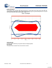
2. Does not meet USB 2.0 specification for D+ and D- rise/fall matching when supply voltage is under 3.3V
n PROBLEM DEFINITION
Rising to falling rate matching of the USB D+ and D- lines has a corner case at lower supply voltages, such
as those under 3.3V.
n PARAMETERS AFFECTED
Rising to falling rate matching of the USB data lines.
n TRIGGER CONDITION(S)
Operating the VCC supply voltage at the low end of the chip’s specification (under 3.3V) may cause a
missmatch in the rising to falling rate.
[+] Feedback


