CY8C24094, CY8C24794
CY8C24894, CY8C24994
Document Number: 38-12018 Rev. *M Page 23 of 47
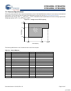
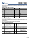
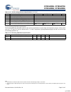
10.3.3 DC Full-Speed USB Specifications
The following table lists guaranteed maximum and minimum specifications for the voltage and temperature ranges: 4.75V to 5.25V
and -10°C ≤ T
A
≤ 85°C, or 3.0V to 3.6V and -10°C ≤ T
A
≤ 85°C, respectively. Typical parameters apply to 5V and 3.3V at 25°C and
are for design guidance only.
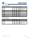
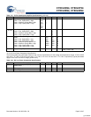
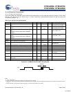
10.3.4 DC Operational Amplifier Specifications
The following tables list guaranteed maximum and minimum specifications for the voltage and temperature ranges: 4.75V to 5.25V
and -40°C ≤ T
A
≤ 85°C, or 3.0V to 3.6V and -40°C ≤ T
A
≤ 85°C, respectively. Typical parameters apply to 5V and 3.3V at 25°C and
are for design guidance only.
The Operational Amplifier is a component of both the Analog Continuous Time PSoC blocks and the Analog Switched Capacitor PSoC
blocks. The guaranteed specifications are measured in the Analog Continuous Time PSoC block.
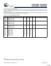
Table 10-6. DC Full-Speed (12 Mbps) USB Specifications
Symbol Description Min Typ Max Units Notes
USB Interface
V
DI
Differential Input Sensitivity 0.2 – – V | (D+) - (D-) |
V
CM
Differential Input Common Mode Range 0.8 – 2.5 V
V
SE
Single Ended Receiver Threshold 0.8 – 2.0 V
C
IN
Transceiver Capacitance – – 20 pF
I
I/O
High-Z State Data Line Leakage -10 – 10 μA0V < V
IN
< 3.3V.
R
EXT
External USB Series Resistor 23 – 25 W In series with each USB pin.
V
UOH
Static Output High, Driven 2.8 – 3.6 V 15 kΩ ± 5% to Ground. Internal pull-up
enabled.
V
UOHI
Static Output High, Idle 2.7 – 3.6 V 15 kΩ ± 5% to Ground. Internal pull-up
enabled.
V
UOL
Static Output Low – – 0.3 V 15 kΩ ± 5% to Ground. Internal pull-up
enabled.
Z
O
USB Driver Output Impedance 28 – 44 W Including R
EXT
Resistor.
V
CRS
D+/D- Crossover Voltage 1.3 – 2.0 V
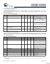
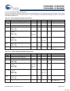
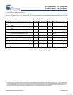
Table 10-7. 5V DC Operational Amplifier Specifications
Symbol Description Min Typ Max Units Notes
V
OSOA
Input Offset Voltage (absolute value)
Power = Low, Opamp Bias = High
Power = Medium, Opamp Bias = High
Power = High, Opamp Bias = High
–1.6
1.3
1.2
10
8
7.5
mV
mV
mV
–
–
TCV
OSOA
Average Input Offset Voltage Drift – 7.0 35.0 μV/
o
C
I
EBOA
Input Leakage Current (Port 0 Analog Pins) – 20 – pA Gross tested to 1 μA.
C
INOA
Input Capacitance (Port 0 Analog Pins) – 4.5 9.5 pF Package and pin dependent. Temp =
25
o
C.
V
CMOA
Common Mode Voltage Range
Common Mode Voltage Range (high power
or high opamp bias)
0.0 – Vdd
Vdd -
0.5
V The common-mode input voltage
range is measured through an analog
output buffer. The specification
includes the limitations imposed by
the characteristics of the analog
output buffer.
0.5 –
G
OLOA
Open Loop Gain
Power = Low, Opamp Bias = High
Power = Medium, Opamp Bias = High
Power = High, Opamp Bias = High
60
60
80
––dB
[+] Feedback


