PRELIMINARY CY8CNP102B, CY8CNP102E
Document #: 001-43991 Rev. *D Page 33 of 38
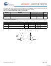
Switching Waveforms
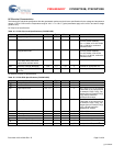
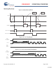
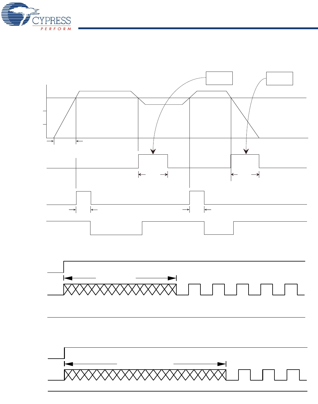
Figure 8. AutoStore/Power Up RECALL
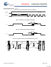
Figure 9. PLL Lock Timing Diagram
Figure 10. PLL Lock for Low Gain Setting Timing Diagram
V
CC
V
SWITCH
t
STORE
t
STORE
t
HRECALL
t
HRECALL
AutoStore
POWER-UP RECALL
Read & Write Inhibited
STORE occurs only
if a SRAM write
has happened
No STORE occurs
without atleast one
SRAM write
t
VCCRISE
24 MHz
F
PLL
PLL
Enable
T
PLLSLEW
PLL
Gain
0
24 MHz
F
PLL
PLL
Enable
T
PLLSLEW LOW
PLL
Gain
1
[+] Feedback


