CYDC256B16, CYDC128B16,
CYDC064B16, CYDC128B08,
CYDC064B08
Document #: 001-01638 Rev. *E Page 7 of 26
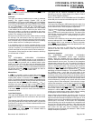
When reading a semaphore, all sixteen/eight data lines output
the semaphore value. The read value is latched in an output
register to prevent the semaphore from changing state during
a write from the other port. If both ports attempt to access the
semaphore within t
SPS
of each other, the semaphore will
definitely be obtained by one side or the other, but there is no
guarantee which side will control the semaphore. On
power-up, both ports should write “1” to all eight semaphores.
Architecture
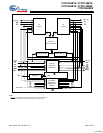
The CYDC256B16, CYDC128B16, CYDC064B16,
CYDC128B08, CYDC064B08 consist of an array of 4k, 8k, or
16k words of 16 dual-port RAM cells, I/O and address lines,
and control signals (CE
, OE, R/W). The CYDC064B08 and
CYDC128B08 consist of an array of 8k and 16k words of 8
each of dual-port RAM cells, I/O and address lines, and control
signals (CE
, OE, R/W).These control pins permit independent
access for reads or writes to any location in memory. To handle
simultaneous writes/reads to the same location, a BUSY pin is
provided on each port. Two Interrupt (INT
) pins can be utilized
for port-to-port communication. Two Semaphore (SEM
)
control pins are used for allocating shared resources. With the
M/S pin, the devices can function as a master (BUSY pins are
outputs) or as a slave (BUSY
pins are inputs). The devices
also have an automatic power-down feature controlled by CE
.
Each port is provided with its own output enable control (OE
),
which allows data to be read from the device.
Notes:
11.This column applies to x16 devices only.
12.See Interrupts Functional Description for specific highest memory locations by device.
13.If BUSY
R
= L, then no change.
14.If BUSY
L
= L, then no change.
15.See Functional Description for specific addresses by device.
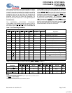
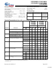
Table 1. Non-Contending Read/Write
Inputs Outputs
OperationCE R/W OE UB LB SEM I/O
8
–I/O
15
[11]
I/O
0
–I/O
7
H X X X X H High Z High Z Deselected: Power-down
X X X H H H High Z High Z Deselected: Power-down
L L X L H H Data In High Z Write to Upper Byte Only
L L X H L H High Z Data In Write to Lower Byte Only
L L X L L H Data In Data In Write to Both Bytes
L H L L H H Data Out High Z Read Upper Byte Only
L H L H L H High Z Data Out Read Lower Byte Only
L H L L L H Data Out Data Out Read Both Bytes
X X H X X X High Z High Z Outputs Disabled
H H L X X L Data Out Data Out Read Data in Semaphore Flag
X H L H H L Data Out Data Out Read Data in Semaphore Flag
H X X X L Data In Data In Write D
IN0
into Semaphore Flag
X X H H L Data In Data In Write D
IN0
into Semaphore Flag
LXXLXL Not Allowed
L X X X L L Not Allowed
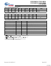
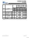
Table 2. Interrupt Operation Example (Assumes BUSY
L
= BUSY
R
= HIGH)
[12]
Function
Left Port Right Port
R/W
L
CE
L
OE
L
A
0L–13L
INT
L
R/W
R
CE
R
OE
R
A
0R–13R
INT
R
Set Right INT
R
Flag L L X 3FFF
[15]
XXXX X L
[14]
Reset Right INT
R
Flag X X X X X X L L 3FFF
[15]
H
[13]
Set Left INT
L
Flag X X X X L
[13]
LLX 3FFE
[15]
X
Reset Left INT
L
Flag X L L 3FFE
[15]
H
[14]
XXX X X
[+] Feedback


