CYDC256B16, CYDC128B16,
CYDC064B16, CYDC128B08,
CYDC064B08
Document #: 001-01638 Rev. *E Page 20 of 26
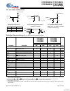
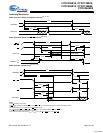
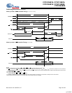
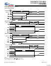
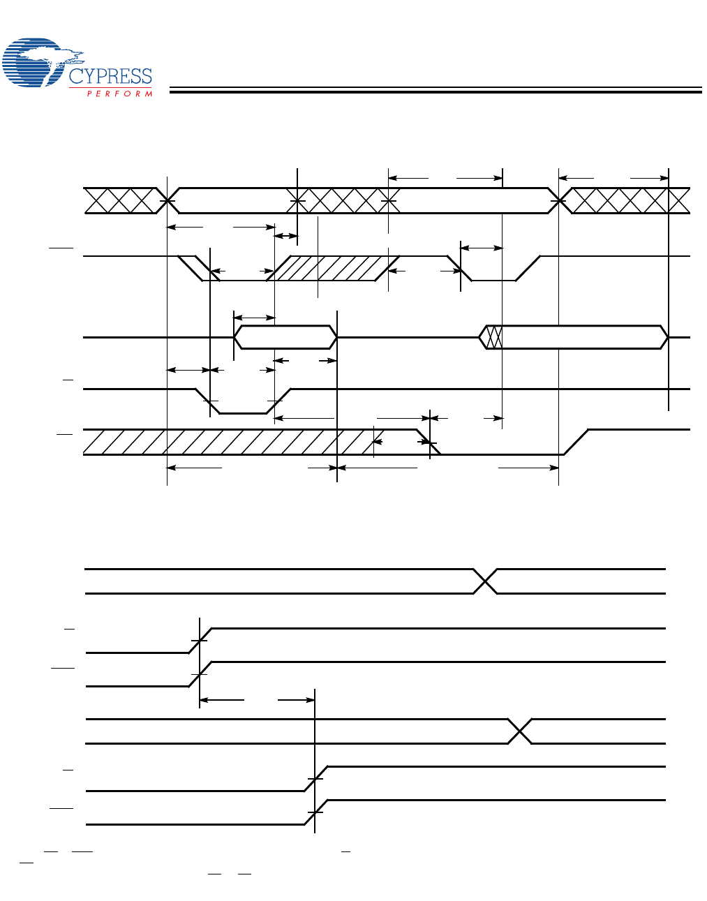
Semaphore Read After Write Timing, Either Side
[49, 50]
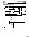
Timing Diagram of Semaphore Contention
[51, 52]
Notes:
49.If the CE
or SEM LOW transition occurs simultaneously with or after the R/W LOW transition, the outputs remain in the high-impedance state.
50.CE
= HIGH for the duration of the above timing (both write and read cycle).
51.I/O
0R
= I/O
0L
= LOW (request semaphore); CE
R
= CE
L
= HIGH.
52.If t
SPS
is violated, the semaphore will definitely be obtained by one side or the other, but which side will get the semaphore is unpredictable.
Switching Waveforms (continued)
t
SOP
t
SAA
VALID ADRESS VALID ADRESS
t
HD
DATA
IN
VALID
t
OHA
t
AW
t
HA
t
ACE
t
SOP
t
SCE
t
SD
t
SA
t
PWE
t
SWRD
t
DOE
WRITE CYCLE READ CYCLE
OE
R/W
I/O
0
SEM
A
0
–A
2
DATA
OUT
VALID
MATCH
t
SPS
MATCH
R/W
L
SEM
L
R/W
R
SEM
R
A
0L
–A
2L
A
0R
–A
2R
[+] Feedback


