


The adjustable range of voltage: -4V ~ +20V (-1,600
LSB
~ +8,000
LSB
)
The adjustable range of current: -8 mA ~ +40 mA (-1,600
LSB
~ +8,000
LSB
)
Please note that: GAIN value – OFFSET value = +400
LSB
~ +6,000
LSB
(voltage or current). When GAIN –
OFFSET is small (steep oblique), the resolution of output signal will be finer and variation on the digital value will
be greater. When GAIN – OFFSET is big (gradual oblique), the resolution of output signal will be rougher and
variation on the digital value will be smaller.
7. CR #30: Error status value (See the table below)
Error status Content b15 ~ b8
b7
b6
b5
b4
b3
b2
b1
b0
Abnormal power supply K1(H’1) 0 0 0 0 0 0 0 1
Incorrect analog input
value
K2(H’2) 0 0 0 0 0 0 1 0
Incorrect mode setting K4(H’4) 0 0 0 0 0 1 0 0
OFFSET/GAIN error K8(H’8) 0 0 0 0 1 0 0 0
Hardware malfunction K16(H’10)
0 0 0 1 0 0 0 0
Abnormal digital range K32(H’20)
0 0 1 0 0 0 0 0
Incorrect average times
setting
K64(H’40)
0 1 0 0 0 0 0 0
Instruction error K128(H’80)
reserved
1 0 0 0 0 0 0 0
Note: Each error status is determined by the corresponding bit (b0 ~ b7) and there may be more than 2 errors occurring at the same time.
0 = normal; 1 = error
8. CR#31: The setting of RS-485 communication address (Range: 01 ~ 255, default = K1).
9. CR#32: The setting of RS-485 communication speed. b0: 4,800bps; b1: 9,600bps (default); b2: 19,200bps; b3:
38,400bps; b4: 57,600bps; b5: 115,200bps; b6 ~ b13: reserved; b14: high/low bit exchange of CRC checksum
(only valid in RTU mode); b15 = 0: ASCII mode; b15 = 1: RTU mode. ASCII data format: 7-bit, Even bit, 1 stop
bit (7, E, 1); RTU data format: 8-bit, Even bit, 1 stop bit (8, E, 1).
10. CR#33: For authorizations on some internal functions, e.g. OFFSET/GAIN tuning. The latched function will
store the output setting in the internal memory before the power is cut off.
11. CR#34: Firmware version of the model.
12. CR#35 ~ CR#48: Parameters for system use.
13. CR#0 ~ CR#34: The corresponding parameter addresses H’4032 ~ H’4054 are for users to read/write data by
RS-485 communication. When using RS-485, the user has to separate the module with MPU first.
a. Communication baud rate: 4,800/9,600/19,200/38,400/57,600/115,200bps
b. Modbus ASCII/RTU communication protocols: ASCII data format (7-bit, Even bit, 1 stop bit (7, E, 1)); RTU
data format (8-bit, Even bit, 1 stop bit (8, E, 1)).
c. Function: H’03 (read register data); H’06 (write 1 word datum to register); H’10 (write many word data to
register)
d. Latched CR should be written by RS-485 communication to stay latched. CR will not be latched if written by
MPU through TO/DTO instruction.
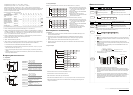
Adjusting D/A Conversion Curve
4.1 Explanation
Voltage Output Mode
+2,000
+4,000
2V
5V
6V
10V
OFFSET
GAIN
V
o
l
t
a
g
e
o
u
t
p
u
t
Digital input
Mode 1
Mode 0
CR#1 mode 0
GAIN = 5V (2,000
LSB
)
OFFSET = 0V (0
LSB
)
CR#1 mode 1
GAIN = 6V (2,400
LSB
)
OFFSET = 2V (800
LSB
)
GAIN
The voltage output value when the digital
input value = K2,000
Range: -4V ~ +20V (-1,600
LSB
~ +8,000
LSB
)
OFFSET
The voltage output value when the digital
input value = K0
Range: -5V ~ +5V (-2,000
LSB
~ +2,000
LSB
)
GAIN - OFFSET Range: +1V ~ +15V (+400
LSB
~ +6,000
LSB
)
Current Output Mode
0
+2,000
+4,000
20mA
OFFSET
GAIN
12mA
10mA
4mA
C
u
r
r
e
n
t
o
u
t
p
u
t
Digital input
Mode 2
Mode 3
CR#1 mode 2
GAIN = 12mA (2,400
LSB
)
OFFSET = 4mA (800
LSB
)
CR#1 mode 3
GAIN = 10mA (2,000
LSB
)
OFFSET = 0mA (0
LSB
)
GAIN
The current output value when the digital
input value = K2,000
Range: -8mA ~ +40mA (-1,600
LSB
~
+8,000
LSB
)
OFFSET
The current output value when the digital
input value = K0
Range: -10mA ~ +10mA (-2,000
LSB
~
+2,000
LSB
)
GAIN - OFFSET
Range: +2mA ~ +30mA (+400
LSB
~ +6,000
LSB
)
4.2 Program Example
Example 1: Set the OFFSET value of CH1as 0V (= K0
LSB
) and GAIN value as 2.5V (= K1,000
LSB
).
X0
K1000
K24
H10 K1
K1
H0
K1
M1002
K33
K1
K1
K18
K0
TO
TO
TO
TO
K1
K1
K1
K1
Write H’10 into CR#1 of analog output module
No.1 and set CH1 in mode 0 (voltage output 0V
~ +10V) and CH2 in mode 2 (current output
4mA ~ +20mA).
Write H’0 into CR#33 and allow OFFSET/GAIN
tuning in CH1 ~ CH4
When X0 goes from Off to On, write the
OFFSET value K0
LSB
into CR#18 and the GAIN
value K1,000
LSB
into CR#24.
Example 2: Set the OFFSET value of CH2 as 2mA (= K400
LSB
) and GAIN value as18mA (= K3,600
LSB
).
X0
K1
K1
H0
K1
M1002
K33
K1
K1
H18
K19
K25
K400
K3600
TO
TO
TO
TO
K1
K1
K1
K1
Write H’18 into CR#1 of analog output module
No.1 and set CH1 in mode 0 (voltage output 0V
~ +10V) and CH2 in mode 3 (current output
0mA ~ +20mA).
Write H’0 into CR#33 and allow OFFSET/GAIN
tuning in CH1 ~ CH4
When X0 goes from Off to On, write the
OFFSET value K400
LSB
into CR#19 and the
GAIN value K3,600
LSB
into CR#25.
Trial Operation & Troubleshooting
LED Display
1. When the module is powered for the first time, POWER LED will be on. After ERROR LED being on for 0.5
second, D/A LED will start to flash.
2. When the power supply is normal, POWER LED will be on and ERROR LED should be off. When the
power supply is less than 19.5V, ERROR LED will keep being on until the power supply is higher than
19.5V.
3. When controlled by RS-485, the RS-485 LED will flash after receiving RS-485 instruction.
4. When the input or output value exceeds the upper bound or falls below the lower bound after conversion,
ERROR LED will flash.
Program Example
M0
K1
M1000
FROM
END
D0
TO
K0K1
D0CMP H6401
INC D100
ADD D101 K5
= K4000 RST
H10
K2K6
M1
M1013
D101
D100
D100
=
K4000
RST
D101
D101
K1
K1
K1
TO
M1
K1
D100
Read the model name from K1 and see if it is DVP04DA-H2: H’6401.
D100 increases K1 and D101 increases K5 every second.
When D100 and D101 reach K4,000, they will be cleared as 0.
See if the model is DVP04DA-H2 when M1 = On. If so, set up output mode: CH1 in mode 0; CH2 in mode 2.
Write the output settings of D100 and D101 into CR#6 and CR#7. The analog output will change with the
changes in D100 and D101.
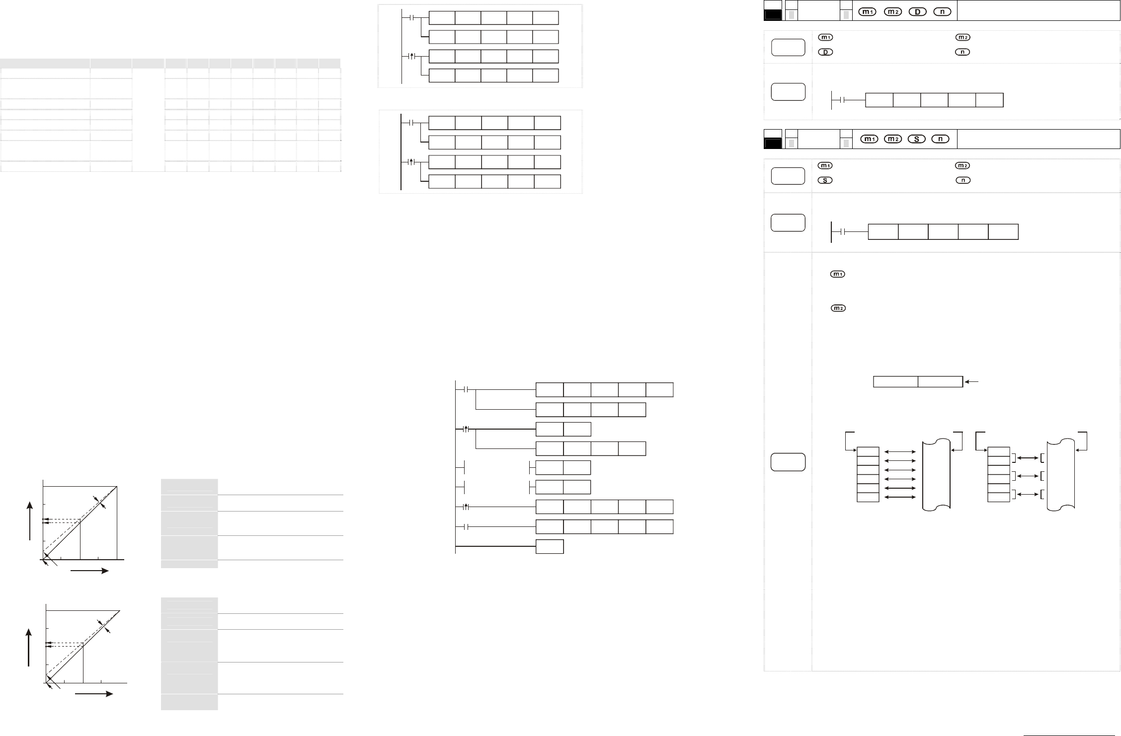
Relevant Instructions
API
78
D
FROM
P
Read CR data in special modules
Instruction
Explanation
: No. of special module (m1 = 0 ~ 7) : CR# in special module to be read
: Device for storing read data : Number of data to be read at a time
Program
Example
Read CR#24 of special module No.0 into D0 and
CR#25 into D1. Only 2 groups of data is read at
a time (n = 2).
X0
FROM K0 K24 D0 K2
API
79
D
TO
P
Write CR data into special modules
Instruction
Explanation
: No. of special module (m1 = 0 ~ 7) : CR# in special module to be written
: Data to be written into CR : Number of data to be written at a time
Program
Example
Use 32-bit instruction DTO to write the content in D11 and D10 into CR#7 and CR#6 of special
module No.0. Only 1 group of data is written in at a time (n = 1).
X0
DTO
K0 K6
D10
K1
Remarks
Operand rules
1.
: The No. of special modules connected to PLC MPU. No. 0 is the module closest to te
MPU. Maximum 8 modules are allowed to connected to a PLC MPU and they will not occupy
any I/O points.
2.
: CR#. CR (control register) is the 49 16-bit memories built in the special module,
numbered in decimal as #0 ~ #48. All operation status and settings of the special module are
contained in the CR.
3. FROM/TO instruction is for reading/writing 1 CR at a time. DFROM/DTO instruction is for
reading/writing 2 CRs at a time.
CR #10 CR #9
Lower 16-bit
Designated CR number
Higher 16-bit
4. Number of groups “n” to be transmitted: n = 2 in 16-bit instructions and n = 1 in 32-bit
instructions mean the same.
D0
D1
D2
D3
D4
D5
CR #5
CR #6
CR #7
CR #8
CR #9
CR #10
D0
D1
D2
D3
D4
D5
CR #5
CR #6
CR #7
CR #8
CR #9
CR #10
Designated device
Designated CR
Designated device
Designated CR
16-bit instruction when n=6
32-bit instruction when n=3
M1083 for switching instruction modes in EH2 series models
1. When M1083 = Off, during the execution of FROM/TO instruction, all external or internal
interruption subroutines will be forbidden. The interruptions are allowed only after FROM/TO
instruction finishes its execution. FROM/TO instruction can also be used in an interruption
subroutine.
2. When M1083 = On and an interruption signal occurs during the execution of FROM/TO
instruction, the interruption will be processed first (with a 100us delay) and the execution of
FROM/TO will be stopped. After the interruption subroutine finishes its execution, the
program will jump to the next instructio of FROM/TO. FROM/TO cannot be used in an
interruption subroutine.
The content of this instruction sheet may be revised without prior notice. Please consult our distributors or
download the most updated version at http://www.delta.com.tw/industrialautomation