


OPEP-33-A4K3R
DELTA ELECTRONICS, INC.
5 Revision: S1
03/12/2007
www.deltaww.com
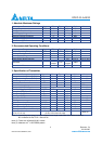
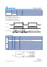
VccT BiasCNT Data Input Optical Output
VccT < 3.1V X X OFF
Low X OFF
No Other
VccT > 3.1V
High
Yes Laser bias and modulation signal output
X = Don’t care
Other = Less than +7.5dBm (peak)
High = Logic high level, Low = logic low level
No = No Data Input, Yes = Data Input,
OFF = Optical Power is less than –45dBm
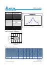
BiasCNT
Optical Output
Within 15% of steady state
Ton Toff
Data Input
L
H
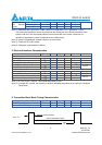
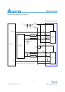
7. Pin Description
Tx/Rx Pin No. I/O Pin Name Description
1
VeeR
Receiver Ground
2
VccR
+3.3V Receiver Power Supply
3 O
SD Normal Optical Input indicated by logic “High”, and No Optical
Input indicated by logic “Low”. (LVTTL)
4 O
RD(n)
Inverted Receiver Data Output (AC-Coupled CML output)
Rx
5 O
RD(p)
Non-Inverted Receiver Data Output (AC-Coupled CML output)
6
VccT
+3.3V Transmitter Power Supply
7
VeeT
Transmitter Ground
8 I
BiasCNT
Positive pulse which control the ONU burst mode operation
9 I
TD(p)
Non-Inverted Transmitter Data Input (AC-Coupled LVPECL input)
Tx
10 I
TD(n)
Inverted Transmitter Data Input (AC-Coupled LVPECL input)
MS
Mounting studs/ connect this pin to Chassis ground
Bottom View
MS
MS