


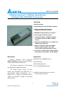

OPEP-33-A4Q1RI
DELTA ELECTRONICS, INC.
6 Revision: S3
12/20/2007
www.deltaww.com
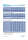
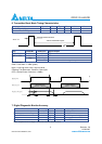
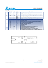
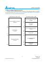
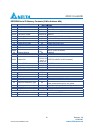
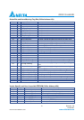
8. Pin Description
Tx/Rx Pin No. I/O Pin Name Description
1
VeeR
Receiver Ground
2
VccR
+3.3V Receiver Power Supply
3 O
SD Normal Optical Input indicated by logic “High”, and No Optical
Input indicated by logic “Low”.
4 O
RD(n)
Inverted Receiver Data Output (AC-Coupled)
Rx
5 O
RD(p)
Non-Inverted Receiver Data Output (AC-Coupled)
6
VccT
+3.3V Transmitter Power Supply
7
VeeT
Transmitter Ground
8 I
BiasCNT
Positive pulse which control the ONU burst mode operation
9 I
TD(p)
Non-Inverted Transmitter Data Input
10 I
TD(n)
Inverted Transmitter Data Input
11
VeeT
Transmitter Ground
12
NC
Not Connect
13 I/O
SDA
I2C Serial Data Input/Output (LVTTL) (Mod-Def 2)
Tx
14 I
SCL
I2C Serial Clock Input (LVTTL) (Mod-Def 1)
MS
Mounting Studs/Connect this pin to Chassis ground
HL
EMI Shielding Leads/ connect this pin to Chassis/ Signal ground