


OPGP-34-A4B3RA
DELTA ELECTRONICS, INC.
5 Revision: S2
12/26/2006
www.deltaww.com
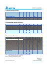
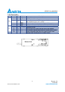
7. Pin Description
Tx/Rx Pin No. I/O Pin Name Description
1
VeeR
Receiver Ground
2
VccR
+3.3V Receiver Power Supply
3 O
SD Normal Optical Input indicated by logic “High”, and No Optical
Input indicated by logic “Low”. (LVTTL)
4 O
RD(n)
Inverted Receiver Data Output (AC-Coupled CML output)
Rx
5 O
RD(p)
Non-Inverted Receiver Data Output (AC-Coupled CML output)
6
VccT
+3.3V Transmitter Power Supply
7
VeeT
Transmitter Ground
8 I
BiasCNT
Positive pulse which control the ONU burst mode operation
9 I
TD(p)
Non-Inverted Transmitter Data Input (DC-Coupled LVPECL input)
Tx
10 I
TD(n)
Inverted Transmitter Data Input (DC-Coupled LVPECL input)
MS
Mounting studs/ connect this pin to Chassis ground
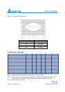
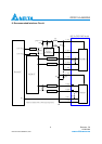
Bottom View
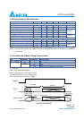
MS
MS