


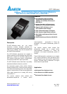

OPT-155Axxxx
DELTA ELECTRONICS, INC.
www.deltaww.com
4
Jan., 2008
Rev. :0F
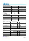
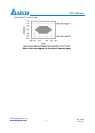
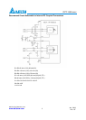
Pin Definition:
PIN Symbol Functional Description
1 GND Receiver Signal Ground
2 RD(+) Receiver Data Out Non-inverted (PECL)
3 RD(-) Receiver Data Out Inverted (PECL)
4 SD Receiver Signal Detect (PECL)
5 VccR Receiver Power Supply
6 VccT Transmitter Power Supply
7 TD(-) Transmitter Data In Inverted (PECL)
8 TD(+) Transmitter Data In Non-inverted (PECL)
9 GND Transmitter Signal Ground
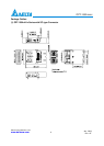
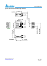
Pin Descriptions:
Pin 1 Receiver Signal Ground, GND
Directly connect these pins to the ground plane.
Pin 2 Receiver Data Out Non-inverted (LVPECL), RD(+)
PECL logic family. Output external biased and internal DC coupled.
Pin 3 Receiver Data Out Inverted (LVPECL), RD ( - )
PECL logic family. Output external biased and internal DC coupled.
Pin 4 Receiver Signal Detect (LVPECL), SD
PECL logic family. Normal Operation: Logic ”1” Output.
Fault Condition: Logic “0” Output.
Pin 5 Receiver Power Supply, VccR
Provide 3.3V/5V DC power supply.
Pin 6 Transmitter Power Supply, VccT
Provide 3.3V/5V DC Power Supply.
Pin 7 Transmitter Data In Inverted (LVPECL), TD(-)
Pin 7 Transmitter Data Input Inverted (LVPECL), TD(-).
Ping 8 Transmitter Data In Non-inverted (LVPECL), TD(+)
Pin 8 Transmitter Data Input Non-inverted (LVPECL), TD(+).
Pin 9 Transmitter Signal Ground, GND
Directly connect these pins to the ground plane.