


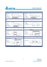
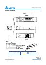

SPBD-155E4J1RT
DELTA ELECTRONICS, INC.
7 Revision: S1
09/20/2006
www.deltaww.com
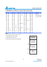
Notes:
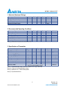
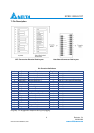
1) Circuit ground is internally isolated from frame (chassis) ground. Tx GND and Rx GND may be internally isolated
within the TRx module.
2) TX Fault is an open collector/drain output, which should be pulled up with a 4.7K~10K resistor on the host board.
Pull up voltage between 2.0V and VccT+0.3V. The output indicates Low when the transmitter is operating
normally, and High with a laser fault including laser end-of-life. In the low state, the output will be pulled to less
than 0.8V.
3) TX disable is an input that is used to shut down the transmitter optical output. It is pulled up within the module
with a 4.7 – 10 K resistor. Its states are:
Low (0 – 0.8V): Transmitter on
(>0.8, < 2.0V): Undefined
High (2.0 – 3.465V): Transmitter Disabled
Open: Transmitter Disabled
4) Mod-Def 0,1,2. These are the module definition pins. They should be pulled up with a 4.7K – 10Kresistor on the
host board. The pull-up voltage shall be VccT or VccR.
Mod-Def 0 is grounded by the module to indicate that the module is present
Mod-Def 1 is the clock line of two-wire serial interface for serial ID
Mod-Def 2 is the data line of two-wire serial interface for serial ID
5) LOS (Loss of Signal) is an open collector/drain output, which should be pulled up with a 4.7K – 10K resistor.
Pull up voltage between 2.0V and VccR+0.3V. When high, this output indicates the received optical power is
below the worst-case receiver sensitivity. Low indicates normal operation. In the low state, the output will be
pulled to less than 0.8V.
6) RD-/+: These are the differential receiver outputs. They are AC coupled 100 differential lines which should be
terminated with 100 (differential) at the user SERDES. The AC coupling is done inside the module and is thus
not required on the host board. The voltage swing on these lines will be between 400 and 2000 mV differential
(200– 1000 mV single ended) when properly terminated.
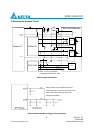
7) VccR and VccT are the receiver and transmitter power supplies. They are defined as 3.3V ±5% at the SFP
connector pin. Recommended host board power supply filtering is shown below page. Inductors with DC
resistance of less than 1 Ohm should be used in order to maintain the required voltage at the SFP input pin with
3.3V supply voltage. When the recommended supply-filtering network is used, hot plugging of the SFP
transceiver module will result in an inrush current of no more than 30 mA greater than the steady state value.
8) TD-/+: These are the differential transmitter inputs. They are AC-coupled, differential lines with 100
differential termination inside the module. The AC coupling is done inside the module and is thus not
required on the host board. The inputs will accept differential swings of 500 – 2400 mV (250 – 1200
mV single-ended), though it is recommended that values between 500 and 1200 mV differential (250 –
600 mV single-ended) be used for best EMI performance.