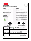
FPF2300/02/03 — Dual-Output Current Limit Switch
© 2009 Fairchild Semiconductor Corporation www.fairchildsemi.com
FPF2300/02/03 • Rev. 1.1.3 4
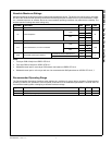
Absolute Maximum Ratings
Stresses exceeding the absolute maximum ratings may damage the device. The device may not function or be opera-
ble above the recommended operating conditions and stressing the parts to these levels is not recommended. In addi-
tion, extended exposure to stresses above the recommended operating conditions may affect device reliability. The
absolute maximum ratings are stress ratings only
.
Notes:
1. Two-layer PCB of 2s0p from JEDEC STD 51-3.
2. Four-layer PBD of 2s0p from JEDEC STD 51-7.
3. Soldered thermal pad on a two-layer PCB without vias based on JEDEC STD 51-3.
4. Soldered thermal pad on a four-layer with two vias connected with GND plane base on JEDEC STD 51-5, 7.
Recommended Operating Range
The Recommended Operating Conditions table defines the conditions for actual device operation. Recommended
operating conditions are specified to ensure optimal performance to the datasheet specifications. Fairchild does not
recommend exceeding them or designing to absolute maximum ratings.
Symbol Parameter Min. Max. Unit
IN, OUTA, OUTB, ONA, ONB, FLAGB(A), FLAGB(B) to GND -0.3 6.0 V
P
D
Power Dissipation
SO8
0.8
(1)
W
1.4
(2)
MLP
0.6
(3)
2.2
(4)
T
STG
Storage Temperature -65 +150 °C
Θ
JA
Thermal Resistance, Junction-to-Ambient
SO8
158
(1)
°C/W
92
(2)
MLP
216
(3)
57
(4)
ESD Electrostatic Discharge Protection
Human Body Model, JESD22-A114 4000
V
Charged Device Model, JESD22-C101 2000
Symbol Parameter Min. Max. Unit
IN Supply Input 1.8 5.5 V
T
A
Ambient Operating Temperature -40 +85 °C


