


www.fairchildsemi.com 4
FSA3357
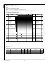
DC Electrical Characteristics (Continued)
Note 4: Measured by the voltage drop between A and B
n
pins at the indicated current through the switch. On Resistance is determined by the lower of the voltages on the two (A
or B
n
Ports).
Note 5: Parameter is characterized but not tested in production.
Note 6: R
ON
= R
ON
max R
ON
min measured at identical V
CC
, temperature and voltage levels.
Note 7: Flatness is defined as the difference between the maximum and minimum value of On Resistance over the specified range of conditions.
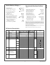
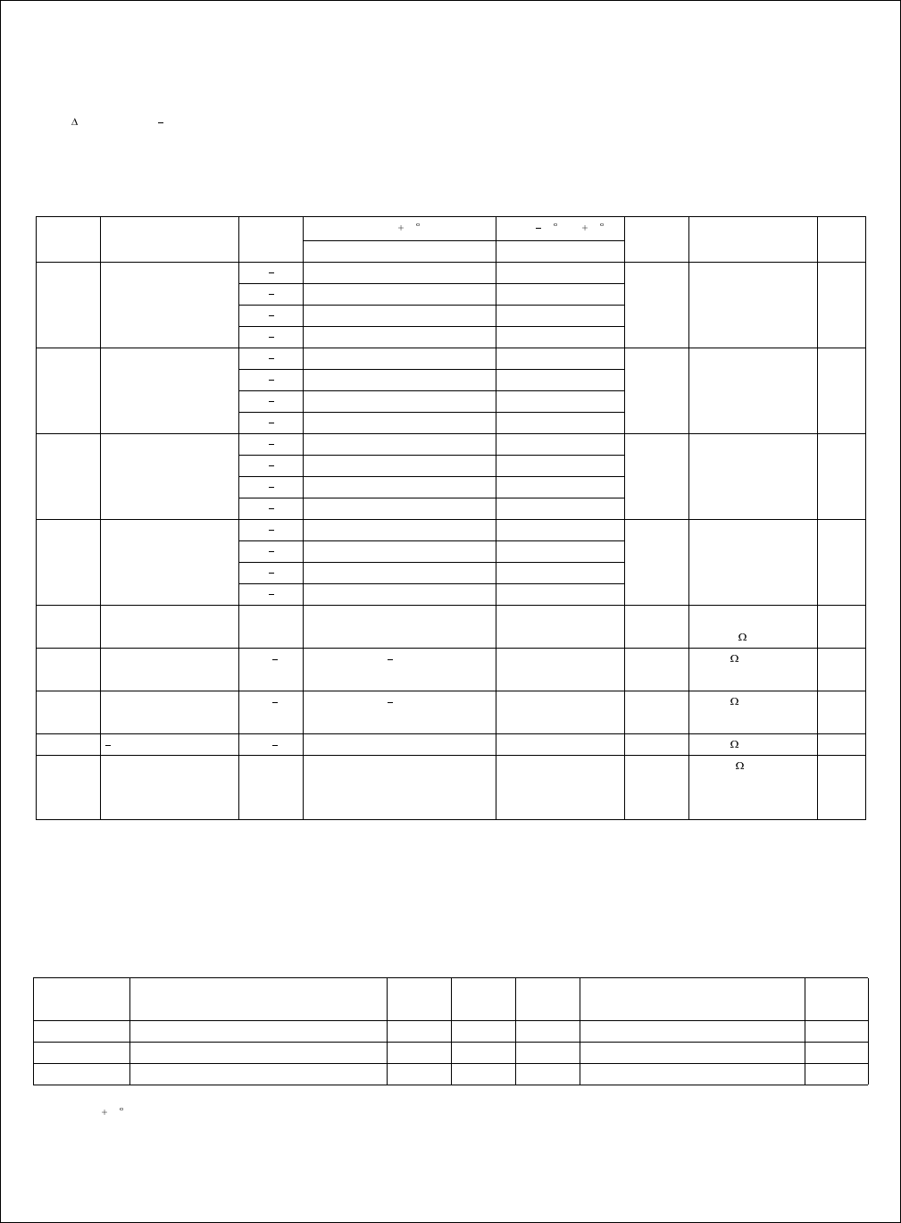
AC Electrical Characteristics
Note 8: This parameter is guaranteed by design but not tested. The bus switch contributes no propagation delay other than the RC delay of the On Resistance of the switch and
the 50 pF load capacitance, when driven by an ideal voltage source (zero output impedance).
Note 9: Guaranteed by Design.
Note 10: Off Isolation = 20 log
10
[V
A
/ V
Bn
]
Capacitance (Note 11)
Note 11: T
A
= 25 C, f = 1 MHz, Capacitance is characterized but not tested in production.
Symbol Parameter
V
CC
T
A
= 25 CT
A
= 40 C to 85 C
Units Conditions
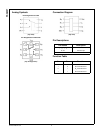
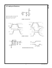
Figure
(V) Min Typ Max Min Max Number
t
PHL
Propagation Delay 1.65 1.95 2.0
ns V
I
= OPEN
Figures
1, 2
t
PLH
Bus to Bus 2.3 2.7 1.1
(Note 8) 3.0 3.6 0.7
4.5 5.5 0.4
t
PZL
Output Enable Time 1.65 1.95 5.0 32.0 5.0 34.0
ns
Figures
1, 2
t
PZH
Turn on Time 2.3 2.7 3.0 15.0 3.0 16.5 V
I
= 2 x V
CC
for t
PZL
(A to B
n
)3.0 3.6 2.0 9.5 2.0 11.0 V
I
= 0V for t
PZH
4.5 5.5 1.5 6.5 1.5 7.0
t
PLZ
Output Disable Time 1.65 1.95 3.0 14.0 3.0 14.5
ns
Figures
1, 2
t
PHZ
Turn Off Time 2.3 2.7 2.0 7.2 2.0 7.8 V
I
= 2 x V
CC
for t
PLZ
(A Port to B
n
Port) 3.0 3.6 1.5 5.1 1.5 5.5 V
I
= 0V for t
PHZ
4.5 5.5 0.8 3.7 0.8 4.0
t
B-M
Break Before Make Time 1.65 1.95 0.5 0.5
ns Figure 3
(Note 9) 2.3 2.7 0.5 0.5
3.0 3.6 0.5 0.5
4.5 5.5 0.5 0.5
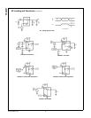
Q Charge Injection (Note 9) 5.0 3.0
pC
C
L
= 0.1 nF, V
GEN
= 0V
Figure 4
3.3 2.0 R
GEN
= 0
OIRR Off Isolation (Note 10) 1.65 5.5 58.0
dB
R
L
= 50
Figure 5
f = 10MHz
Xtalk Crosstalk 1.65 5.5 60.0
dB
R
L
= 50
Figure 6
f = 10MHz
BW 3dB Bandwidth 1.65 5.5 250.0 MHz R
L
= 50 Figure 9
THD Total Harmonic Distortion
5.0 .01 %
R
L
= 600
(Note 9) 0.5 V
P-P
f = 600 Hz to 20 KHz
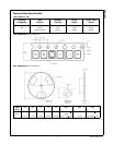
Symbol Parameter Typ Max Units Conditions
Figure
Number
C
IN
Control Pin Input Capacitance 2.0 pF V
CC
= 0V
C
IO-B
B Port Off Capacitance 3.6 pF V
CC
= 5.0V Figure 7
C
IOA-ON
A Port Capacitance When Switch Is Enabled 14.5 pF V
CC
= 5.0V Figure 8