


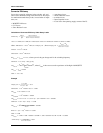
AN50 APPLICATION NOTE
2
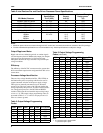
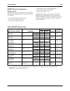
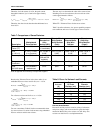
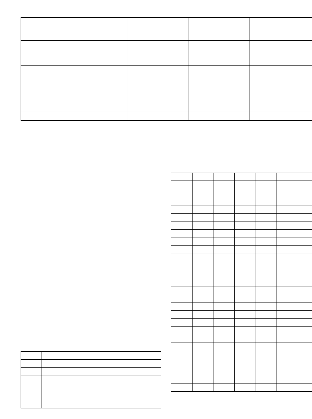
Table 2. Intel Pentium Pro and OverDrive
®
Processor Power Specifications
Notes:
1. Maximum power values are measured at typical V
CC
P to take into account the thermal time constant of the CPU package.
2. Flexible motherboard specifications are recommendations only. Actual specifications are subject to change.
CPU Model, Features
Voltage
Specification,
V
CC
P (VDC)
Maximum
Current,
I
CC
P (A)
Maximum Thermal
Design power
1
(W)
150MHz, 256K L2 Cache 3.1 ±5% 9.9 29.2
166MHz, 512K L2 Cache 3.3 ±5% 11.2 35.0
180MHz, 256K L2 Cache 3.3 ±5% 10.1 31.7
200MHz, 256K L2 Cache 3.3 ±5% 11.2 35.0
200MHz, 512K L2 Cache 3.3 ±5% 12.4 37.9
OverDrive Processors
150Mhz
180Mhz
200Mhz
2.5 ±5% 11.2
12.5
13.9
26.7
29.7
32.9
Flexible Motherboard
2
2.4-3.5 ±5% 14.5 45.0
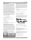
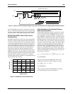
Output Ripple and Noise
Ripple and noise are defined as periodic or random signals
over the frequency band of 20Mhz at the output pins. Output
ripple and noise requirements of ±13mV must be met
throughout the full load range and under all specified input
voltage conditions.
Efficiency
The efficiency of the DC-DC converter must be greater than
80% at maximum output current and greater than 40% at low
current draw.
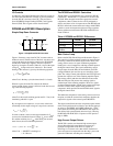
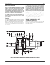
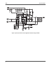
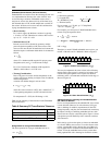
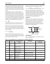
Processor Voltage Identification
There are four voltage identification Pins, VID3-VID0, on
the Pentium Pro processor package which can be used to
support automatic selection of the power supply voltage.
These pins are internally unconnected or are shorted to
ground (V
SS
). The logic status of the VID pins defines the
voltage required by the processor. In order to address future
low voltage microprocessors, the RC5050 and RC5051
include a VID4 input bit to extend the output voltage range
as low as 1.3V. The output voltage programming codes are
presented in Table 3. A “1” refers to an open pin and a ‘0’
refers to a short to ground.
Note:
1. 0 = processor pin is tied to GND
1 = processor pin is open.
Table 3. Output Voltage Programming
Codes
VID4 VID3 VID2 VID1 VID0 V
OUT
to CPU
0 1 1 1 1 1.30V
0 1 1 1 0 1.35V
0 1 1 0 1 1.40V
0 1 1 0 0 1.45V
0 1 0 1 1 1.50V
0 1 0 1 0 1.55V
0 1 0 0 1 1.60V
0 1 0 0 0 1.65V
0 0 1 1 1 1.70V
0 0 1 1 0 1.75V
0 0 1 0 1 1.80V
0 0 1 0 0 1.85V
0 0 0 1 1 1.90V
0 0 0 1 0 1.95V
0 0 0 0 1 2.00V
0 0 0 0 0 2.05V
1 1 1 1 1 No CPU
1 1 1 1 0 2.1V
1 1 1 0 1 2.2V
1 1 1 0 0 2.3V
1 1 0 1 1 2.4V
1 1 0 1 0 2.5V
1 1 0 0 1 2.6V
1 1 0 0 0 2.7V
1 0 1 1 1 2.8V
1 0 1 1 0 2.9V
1 0 1 0 1 3.0V
1 0 1 0 0 3.1V
1 0 0 1 1 3.2V
1 0 0 1 0 3.3V
1 0 0 0 1 3.4V
1 0 0 0 0 3.5V
Table 3. Output Voltage Programming
Codes
(continued)
VID4 VID3 VID2 VID1 VID0 V
OUT
to CPU