


4-8 C141-E166
4.2 Power Supply Requirements
(1) Allowable input voltage and current
The power supply input voltage measured at the power supply connector pin of the IDD (receiving
end) must satisfy the requirement given in Subsection 2.1.3. (For other requirements, see Items (4)
and (5) below.)
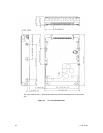
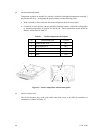
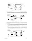
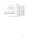
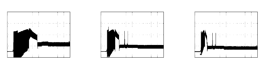
(2) Current waveform (reference)
Figure 4.8 shows the waveform of +12 VDC.
MAP3147 series
Current(500mA/div)
Time(2 sec/div)
MAP3367 series
Current(500mA/div)
MAP3735 series
Current(500mA/div)
Time(2 sec/div) Time(2 sec/div)
Figure 4.8 Current waveform (+12 VDC)
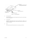
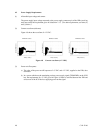
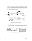
(3) Power on/off sequence
a) The order of the power on/off sequence of +5 VDC and +12 VDC, supplied to the IDD, does
not matter.
b) In a system which uses the terminating resistor power supply signal (TERMPWR) on the SCSI
bus, the requirements for +5 VDC given in Figure 4.9 must be satisfied between the IDD and
at least one of the SCSI devices supplying power to that signal.