MB3878
12
■
■■
■
FUNCTIONAL DESCRIPTION
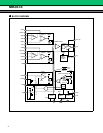
1. DC/DC Converter Unit
(1) Reference voltage block (Ref)
The reference voltage generator uses the voltage supplied from the VCC terminal (pin 18) to generate a tem-
perature-compensated, stable voltage (5.0V Typ) used as the reference supply voltage for the IC’s internal
circuitry.
This pin can also be used to obtain a load current to a maximum of 1mA from the reference voltage VREF
terminal (pin 6).
(2) Triangular wave oscillator block (OSC)
The triangular wave oscillator builds the capacitor for frequency setting into, and generates the triangular wave
oscillator waveform by connecting the frequency setting resistor with the RT terminal (pin 17).
The triangular wave is input to the PWM comparator on the IC.
(3) Error amplifier block (Error Amp.1)
This amplifier detects the output signal from the current detector ampifier (Current amp .1), compares this to the
+INE1 terminal (pin 9), and outputs a PWM control signal to be used in controlling the charging current.
In addition, an arbitrary loop gain can be set up by connecting a feedback resistor and capacitor between the
FB1 terminal (pin 7) and -INE terminal (pin 8), providing stable phase compensation to the system.
(4) Error amplifier block (Error Amp.2)
This amplifier (Error Amp.2) detects voltage pendency of the AC adaptor and outputs a PWM control signal.
In addition, an arbitrary loop gain can be set by connecting a feedback resistor and capacitor from the FB2
terminal (pin 5) to the -INE2 terminal (pin 4) of the error amplifier, enabling stable phase compensation to the
system.
(5) Error amplifier block (Error Amp.3)
This error amplifier (Error Amp. 3) detects the output voltage from the DC/DC converter and outputs the PWM
control signal. External output voltage setting resistors can be connected to the error amplifier inverse input pin
to set the desired level of output voltage from 1 cell to 4 cells.
In addition, an arbitrary loop gain can be set by connecting a feedback resistor and capacitor from the FB3
terminal (pin 15) to the −INE3 terminal (pin 16) of the error amplifier, enabling stable phase compensation to the
system.
Connecting a soft-start capacitor to the CS terminal (pin 22) prevents surge currents when the IC is turned on.
Using an error amplifier for soft-start detection makes the soft-start time constant, independent of the output load.
(6) Current detector amplifier block (Current Amp.1)
The current detection amplifier (Current Amp.1) detects a voltage drop which occurs between both ends of the
output sense resistor (R
S) due to the flow of the charge current, using the +INC1 terminal (pin 13) and
−INC1 terminal (pin 12). Then it outputs the signal amplified by 25 times to the error amplifier (Error Amp.1) at
the next stage.


