


C141-E034-02EN4 - 10
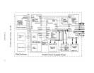
4.6 Read/write Circuit
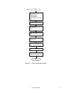
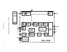
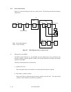
The read/write circuit consists of the read/write preamplifier (PreAMP), the write circuit, the read
circuit, and the time base generator in the read channel (RDC). Figure 4.4 is a block diagram of
the read/write circuit.
4.6.1 Read/write preamplifier (PreAMP)
One PreAMP is mounted on the FPC. The PreAMP consists of an 6-channel read preamplifier and
a write current switch and senses a write error. Each channel is connected to each data head. The
head IC switches the heads by the chip select signals (*CS) and the head select signals (HS0, HS1,
HS2). The IC generates a write error sense signal (WUS) when a write error occurs due to head
short-circuit or head disconnection.
4.6.2 Write circuit
The write data is output from the hard disk controller (HDC) with the NRZ data format, and sent to
the encoder circuit in the RDC with synchronizing with the write clock. The NRZ write data is
converted from 8-bit data to 9-bit data by the encoder circuit then sent to the PreAMP, and the data
is written onto the media.
(1) 8/9 GCR
The disk drive converts data using the 8/9 (0, 4, 4) group coded recording (GCR) algorithm. This
code format is 0 to 4 code bit "0"s are placed between "1"s.
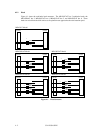
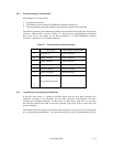
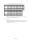
(2) Write precompensation
Write precompensation compensates, during a write process, for write non-linearity generated at
reading. Table 4.2 shows the write precompensation algorithm.
Table 4.2 Write precompensation algorithm
Bit Bit Bit Compensation
n – 1 n n + 1 Bit n
0 1 1 None
1 1 0 Late
1 1 0 Late
Late: Bit is time shifted (delayed) from its nominal time position towards the bit
n+1 time position.