


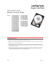
Hitachi Global Storage Technologies
Page 4 version 1.0
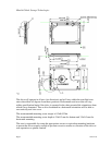
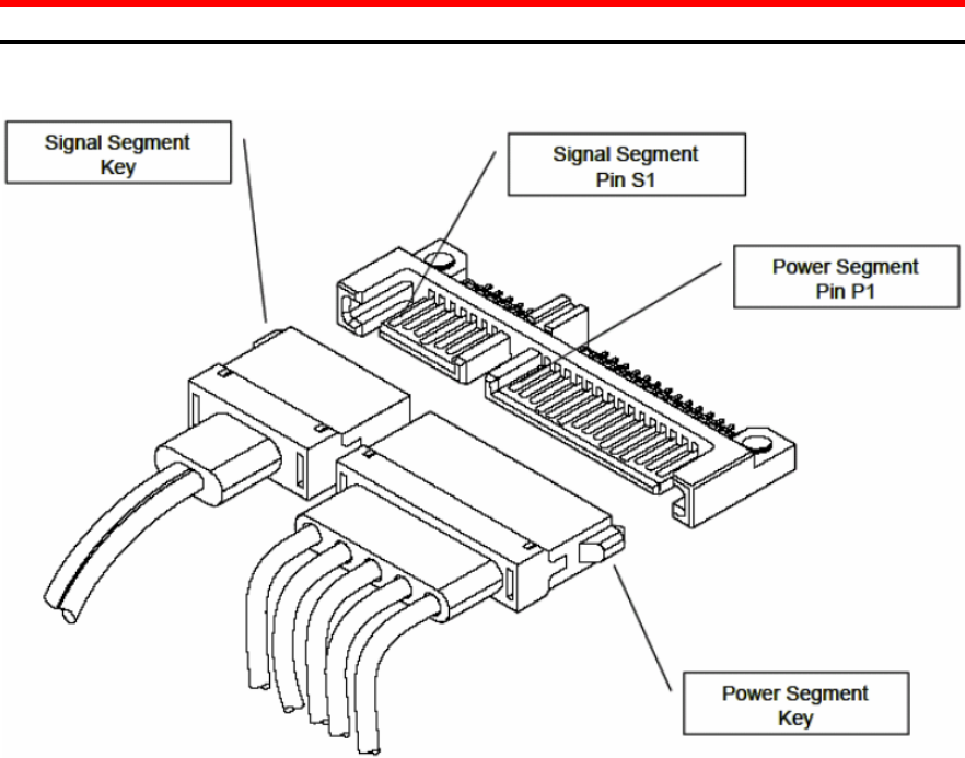
Interface connector
The figure below shows the physical pin location
All pins are in a single row, with a 127 mm (0.050”) pitch.
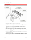
The comments on the mating sequence in Table in the section 7.3 apply to the case of
back-plane
blind-mate connector only. In this case, the mating sequences are:(1)the ground pins
P4 and P12;(2) the pre-charge power pins and the other ground pins; and (3) the
signal pins and the rest of the power pins.
There are three power pins for each voltage. One pin from each voltage is used for
pre-charge in the backplane blind-mate situation.
If a device uses 3.3V, then all V33 pins must be terminated. Otherwise, it is optional
to terminate any of the V33 pins
If a device uses 5.0V, then all V5 pins must be terminated. Otherwise, it is optional to
terminate any of the V5 pins
If a device uses 12.0V, then all V12 pins must be terminated. Otherwise, it is optional
to terminate any of the V12 pins.