


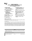
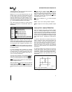

AUTOMOTIVE 80C51FA/83C51FA
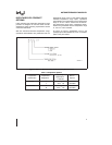
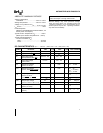
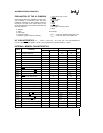
DC CHARACTERISTICS: (T
A
eb
40
Cto
a
125
C; V
CC
e
5V
g
10%; V
SS
e
0V) (Continued)
Symbol Parameter Min Typ Max Unit Test Conditions
I
TL
Logical 1 to 0 Transition Current
b
265
b
650 mAV
IN
e
2V
(Ports 1, 2, and 3)
RRST RST Pulldown Resistor 40 100 225 KX
CIO Pin Capacitance 10 pF
1MHz, 25
C
I
CC
Power Supply Current: (Note 3)
Running at 12 MHz (Figure5) 40 mA
Idle Mode at 12 MHz (Figure5) 15 mA
Power Down Mode (I
PD
) 150 mA
NOTES:
1. Capacitive loading on Ports 0 and 2 may cause noise pulses to be superimposed on the V
OL
s of ALE and Ports 1 and 3.
The noise is due to external bus capacitance discharging into the Port 0 and Port 2 pins when these pins make 1 to 0
transitions during bus operations. In applications where capacitance loading exceeds 100 pFs, the noise pulse on the ALE
signal may exceed 0.8V. In these cases, it may be desirable to qualify ALE with a Schmitt Trigger, or use an Address Latch
with a Schmitt Trigger Strobe input.
2. Capacitive loading on Ports 0 and 2 cause the V
OH
on ALE and PSEN to drop below the 0.9 V
CC
specification when the
address lines are stabilizing.
3. See Figures 6±9 for test conditions. Minimum V
CC
for Power Down is 2.0V.
4. Typicals are based on limited number of samples, and are not guaranteed. The values listed are at room temperature and
5.0V.
5. Under steady state (non-transient) conditions, I
OL
must be externally limited as follows:
MaximumI
OL
per Port Pin: 10 mA
MaximumI
OL
per 8-Bit Port-
Port 0: 26mA
Ports 1,2, and 3: 15mA
MaximumTotal I
OL
for all Output Pins: 71 mA
If I
OL
exceeds the test condition, V
OL
may exceed the related specification. Pins are not guaranteed to sink current greater
than the listed test conditions.
6. Contact Intel for design-in information.
8