


BIOS SETUP
36 MB886 User’s Manual
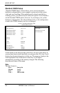
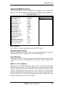
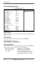
Advanced Chipset Features
This Setup menu controls the configuration of the chipset.
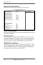
Phoenix - AwardBIOS CMOS Setup Utility
Advanced Chipset Features
DRAM Timing Selectable By SPD ITEM HELP
CAS Latency Time 4 Menu Level >
DRAM RAS# to CAS# Delay 4
DRAM RAS# Precharge 4
Precharge delay (tRAS) 12
System Memory Frequency 533MHZ
SLP_S4# Assertion Width 1 to 2 Sec
System BIOS Cacheable Enabled
Video BIOS Cacheable Disabled
Memory Hole at 15M-16M Disabled
PCI Express Root Port Func Press Enter
** On-Chip VGA Setting **
PEG/On Chip VGA Control Auto
PEG Force x1 Disabled
On-Chip Frame Buffer Size 8MB
DVMT Mode DVMT
DVMT/FIXED memory Size 128MB
Onboard PCU-E LAN Enable
Onchip ICH7 LAN Enable
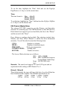
DRAM Timing Selectable
This option refers to the method by which the DRAM timing is selected.
The default is By SPD.
CAS Latency Time
You can configure CAS latency time in HCLKs as 2 or 2.5 or 3. The
system board designer should set the values in this field, depending on
the DRAM installed. Do not change the values in this field unless you
change specifications of the installed DRAM or the installed CPU.
DRAM RAS# to CAS# Delay
This option allows you to insert a delay between the RAS (Row Address
Strobe) and CAS (Column Address Strobe) signals. This delay occurs
when the SDRAM is written to, read from or refreshed. Reducing the
delay improves the performance of the SDRAM.